Universal chip test system and test method and storage medium

A chip test and chip technology, applied in the field of chip verification and testing, can solve the problems of slow construction of chip test systems and inability to share test hardware resources, so as to facilitate the rapid establishment of test systems, improve construction efficiency, and improve test efficiency.

Active Publication Date: 2020-08-04
SHANGHAI HUALI MICROELECTRONICS CORP
View PDF17 Cites 9 Cited by
  • Summary
  • Abstract
  • Description
  • Claims
  • Application Information

AI Technical Summary

Problems solved by technology

[0011] The purpose of the present invention is to provide a general chip test system, test method and storage medium, to solve the problem of inability to share test hardware resources before and after chip tape-out, chip function evaluation, chip performance evaluation, chip Reliability evaluation and other chip test systems are slow to build and cannot be used universally

Method used


Image

  • Universal chip test system and test method and storage medium
  • Universal chip test system and test method and storage medium
  • Universal chip test system and test method and storage medium

Examples


Embodiment 1

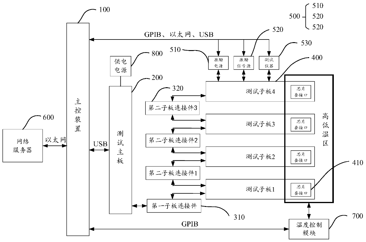
[0080] This embodiment provides a general chip test system, as attached figure 1 As shown, it includes a main control device 100 , a test main board 200 , N sub-board connectors 300 , several test sub-boards 400 and several test suites 500 , where N≥1. In particular, for ease of understanding and illustration, N=4, obviously, this is not a limitation of the present invention.

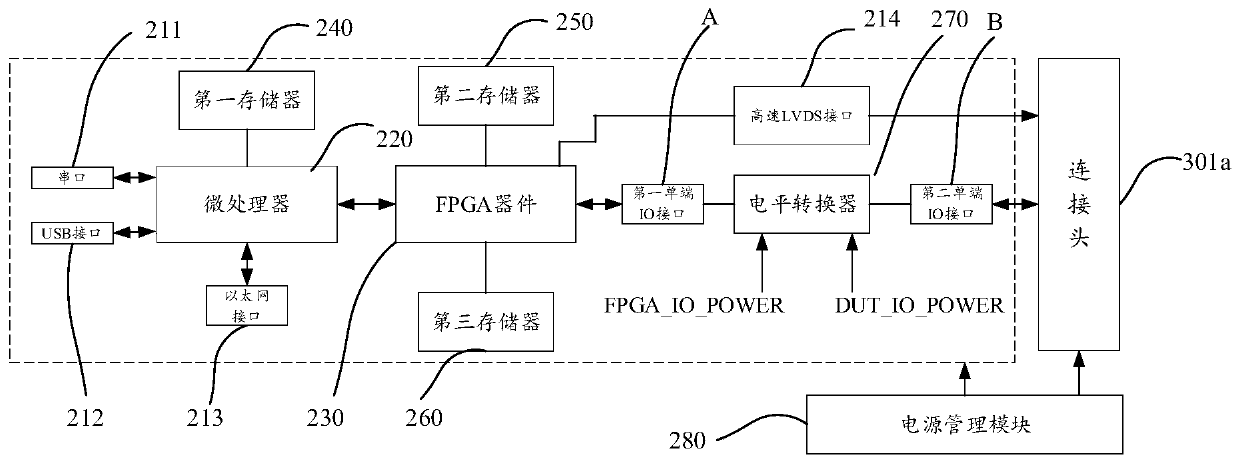
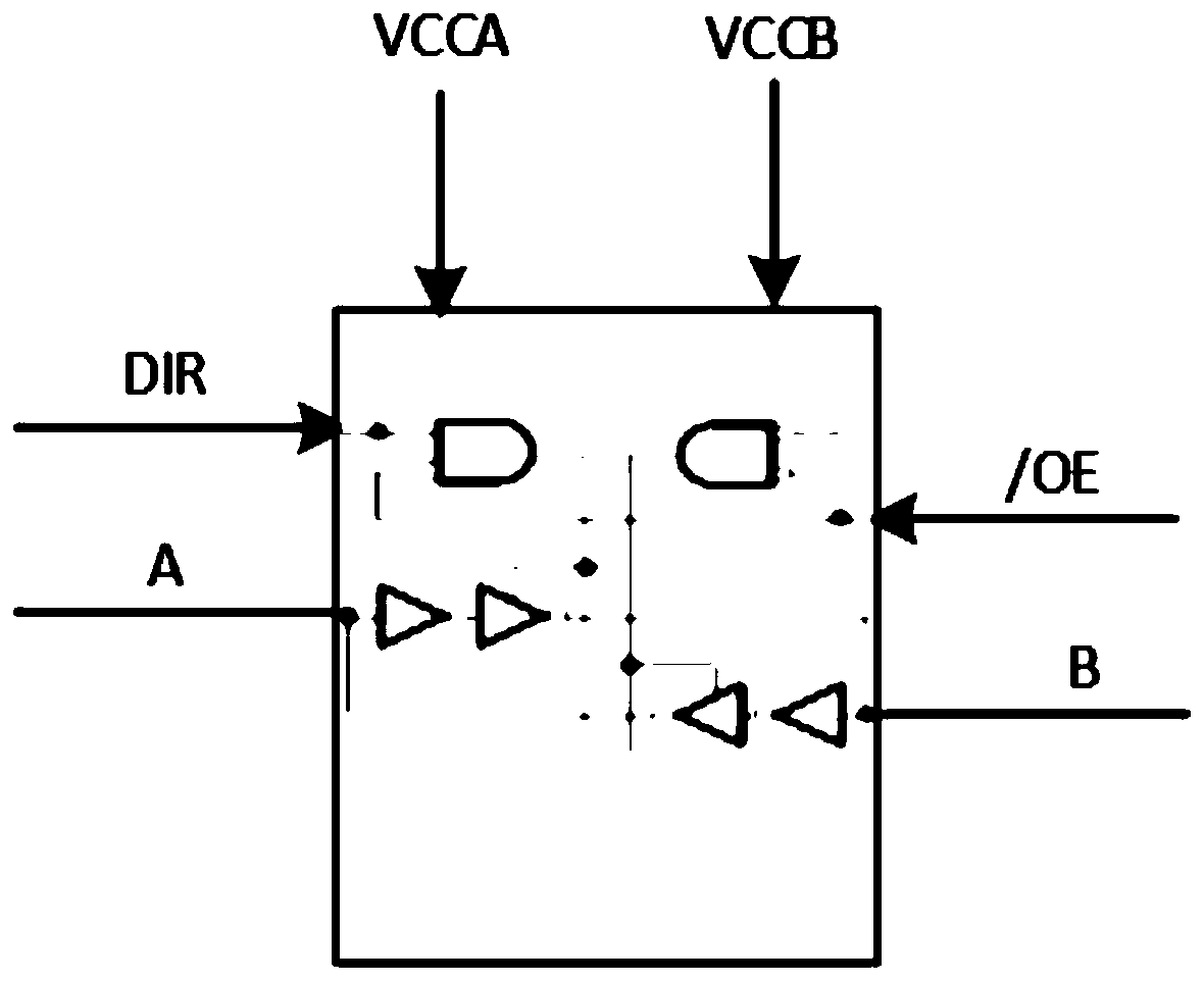
[0081] The main control device 100 is respectively connected to the test main board 200 and several test suites 500, and the N sub-board connectors include a first sub-board connector 310 and N-1 second sub-board connectors. 320, the test main board 200 is connected to the test sub-board 400 through the first sub-board connector 310, the test sub-boards 400 are connected through the second sub-board connector 320, and the first Signals are communicated between a sub-board connector 310 and the second sub-board connector 320 and between the second sub-board connectors 320 . The test sub-board 400 is co...

Embodiment 2

[0112] Based on a general chip testing system provided by any of the above implementations, the embodiment of the present invention provides a general chip testing method, see the attached Figure 9 , including the following steps,

[0113] S100: Receive test configuration information.

[0114] S200: Convert the test configuration information into incentive instructions and test instructions.

[0115] S300: According to the test stimulus, control the test main board, the test sub-board and the chip to be tested to execute the test instruction.

[0116] Preferably, before step S100, the following steps are also included, according to the test configuration information, connecting the test main board and the test suite with the main control device; connecting the test sub-board with the sub-board connector, and connecting the sub-board The board is connected with the test main board; the test suite is connected with the test sub-board, and the chip to be tested is fixed on the...


PUM


Abstract

The invention provides a universal chip test system, a universal chip test method and a storage medium. The chip test system comprises a main control device, a test mainboard, N daughter board connecting pieces, a plurality of test daughter boards and a plurality of test suites. The test mainboard is connected with the main control device, the test suites and the test daughter boards; the test daughter boards match the test suites, and the test daughter boards are connected with the test mainboard through daughter board connecting pieces. The universal chip test system provided by the invention can quickly and accurately verify and test functions and performances before and after chip design, can meet test tasks of function verification, performance test and reliability test before chip manufacturing, adopts a modular design, is high in expandability, and test automation can be realized.

Description

technical field [0001] The invention relates to the technical field of chip verification testing, in particular to a general chip testing system, testing method and storage medium. Background technique [0002] As we all know, the rapid development and continuous innovation of information technology and integrated circuit technology, especially the wide application in the Internet of Things, artificial intelligence, unmanned driving, 5G and other technology industries, has brought great convenience to people's work and life and comfort. Correspondingly, people's pursuit of higher quality of work and life has also promoted the continuous development of integrated circuit technology in the direction of high precision, high speed and high reliability. [0003] The manufacturing process of integrated circuits can usually be divided into wafer manufacturing process, wafer testing, packaging and final testing. Generally, a wafer refers to a silicon wafer used to make an integrat...

Claims


Application Information

Patent Timeline
Patent Type & Authority Applications(China)
IPC IPC(8): G01R31/28
CPCG01R31/2853G01R31/2893G01R31/2855
Inventor 程景全宿晓锋郭婷武建宏
Owner SHANGHAI HUALI MICROELECTRONICS CORP
Why Eureka
Try Eureka