Output circuit of power amplifier

A power amplifier and output circuit technology, applied in the field of power amplifier output circuit, can solve problems such as poor bandwidth performance, limited application range, and limited power amplifier performance, so as to reduce size, space and cost, and improve radio frequency bandwidth and efficiency , Expand the effect of video bandwidth

Active Publication Date: 2020-08-07
INNOGRATION SUZHOU
View PDF4 Cites 3 Cited by
  • Summary
  • Abstract
  • Description
  • Claims
  • Application Information

AI Technical Summary

Problems solved by technology

[0006] The above two implementation methods have certain limitations, and good performance cannot be achieved in some specific occasions. In addition, the existing above two implementation methods also have the following defects:
This greatly limits its scope of application
At the same time, due to the large inductance between the chip capacitor to the ground and the microfarad (uF) level power filter capacitor on the drain bias line, the video bandwidth of the power amplifier is narrowed
In addition, the bonding wire inductance cross combination produces a large mutual inductance, which affects the bandwidth and efficiency of the power amplifier.
[0008] image 3 , 4 In the way of using low-pass matching network to absorb the drain-source capacitance, its own bandwidth performance is not good, and the performance of the power amplifier is very limited.
At the same time, there is also a large inductance between the first ground capacitor and the power filter capacitor of the order of microfarads (uF) on the drain bias line, resulting in narrowing of the video bandwidth of the power amplifier.

Method used


Image

  • Output circuit of power amplifier
  • Output circuit of power amplifier
  • Output circuit of power amplifier

Examples


Embodiment Construction

[0039] The above solution will be further described below in conjunction with specific embodiments. It should be understood that these examples are used to illustrate the present invention and not to limit the scope of the present invention. The implementation conditions used in the examples can be further adjusted according to the conditions of specific manufacturers, and the implementation conditions not indicated are usually the conditions in routine experiments.

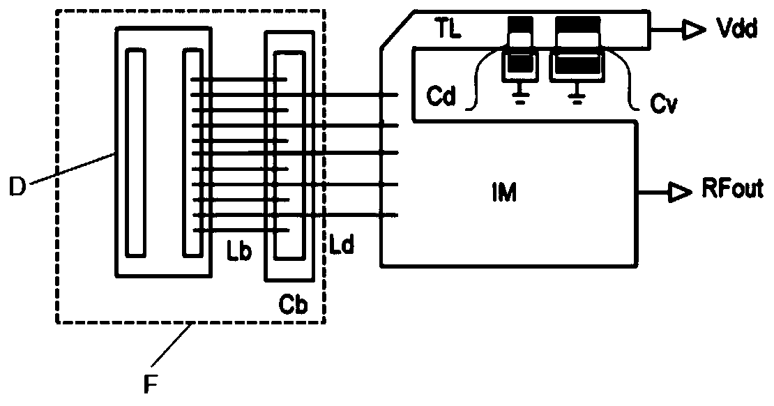
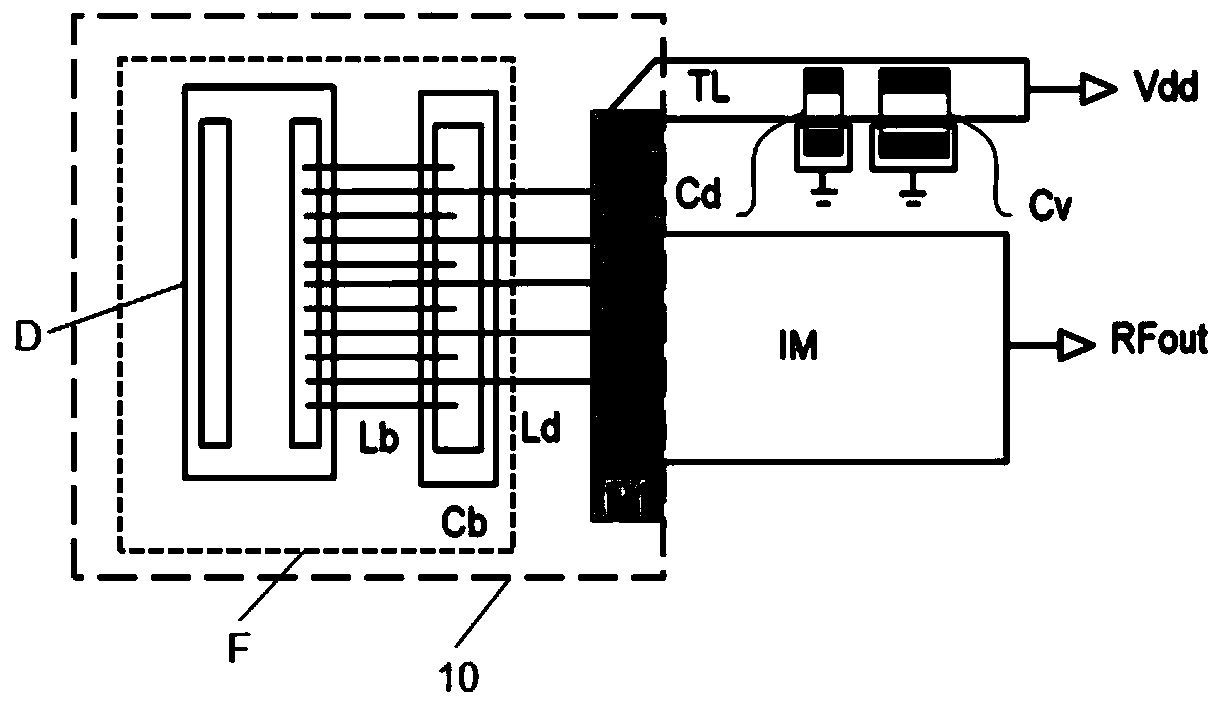
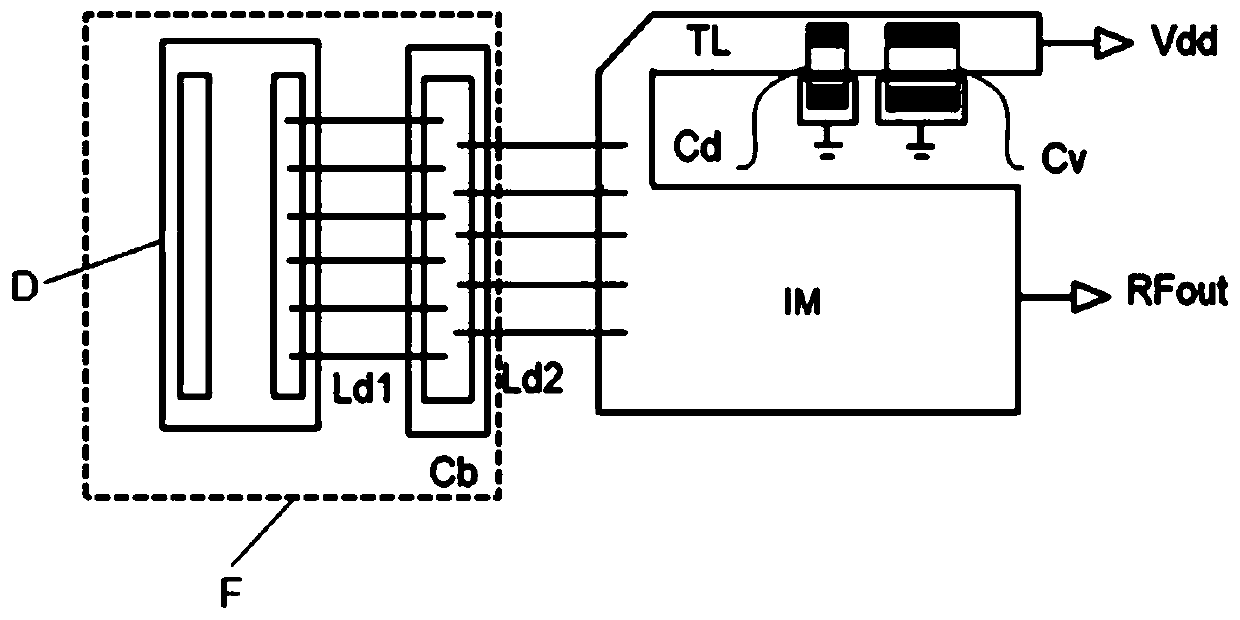
[0040] In the first embodiment, as Figure 5 , 6 As shown, an output circuit of a power amplifier includes:

[0041] An output network OMN connected to active devices, which may include tubes, transistors, integrated circuits, etc. In this embodiment, an active transistor is taken as an example for description.

[0042] The output network OMN includes an impedance matching network IM, and a bias balancing network BCN1.

[0043] The bias balance network BCN1 includes a first ground capacitor Cb1 connected to ...


PUM


Abstract

The invention discloses an output circuit of a power amplifier, comprising an output network connected with an active device, the output network comprising an impedance matching network and a bias balance network; the bias balance network is connected with the output end of the active device chip through a first bonding wire group; the impedance matching network is connected with the output end ofthe active device chip through a second bonding wire group; the bias balance network comprises a first grounding capacitor connected with a transmission line, and the first bonding wire group is connected with one end of the transmission line; an equivalent inductor between the output end of the active device chip and the first grounding capacitor and a drain-source parasitic capacitor of the active device form a first resonance circuit. The transmission line, the bonding line group and the drain-source parasitic capacitance of the active device form a resonance circuit, so that the drain-source parasitic capacitance of the active device is balanced, elements of a matching network are reduced, and the size space and the cost of the amplifier are reduced.

Description

technical field [0001] The invention relates to a power amplifier circuit, in particular to an output circuit of the power amplifier. Background technique [0002] RF power amplifiers are key components at the transmitter end of communication base station systems. The competition in the communication market is becoming more and more fierce, and new requirements are put forward for the key component power amplifier: such as large bandwidth, high power, high efficiency and miniaturization. [0003] At the same time, the RF power amplifiers in the communication base station system generally have relatively large power levels, such as several watts to several hundred watts. Therefore, the physical gate length of the active transistors in this type of power amplifier is also relatively large, which leads to large parasitic parameters of the transistor, such as drain-source capacitance. Since the power amplifier generally needs to be matched and output to the 50Ohm system, a lar...

Claims


Application Information

Patent Timeline
Patent Type & Authority Applications(China)
IPC IPC(8): H03F3/20H03F3/189
CPCH03F3/20H03F3/189Y02D30/70
Inventor 张勇
Owner INNOGRATION SUZHOU
Why Eureka
Try Eureka