BOX-shaped silicon nitride waveguide and preparation method thereof

A technology of forming silicon nitride and silicon nitride, which is applied in the field of BOX-shaped silicon nitride waveguide and its preparation, can solve the problems of insufficiently steep sidewalls, low verticality, and time-consuming, so as to reduce the sidewalls. Scatter loss, reduce process links, improve the effect of smoothness

Active Publication Date: 2020-08-11
GUIYANG UNIV
View PDF11 Cites 1 Cited by
  • Summary
  • Abstract
  • Description
  • Claims
  • Application Information

AI Technical Summary

Problems solved by technology

However, the side walls obtained by directly digging grooves on silicon dioxide are not steep enough, the verticality is not high, the bottom and sides are not flat enough, and most of the groove depth is controlled by RIE etching technology, w

Method used


Image

  • BOX-shaped silicon nitride waveguide and preparation method thereof
  • BOX-shaped silicon nitride waveguide and preparation method thereof
  • BOX-shaped silicon nitride waveguide and preparation method thereof

Examples


Example Embodiment

[0052] Example 1

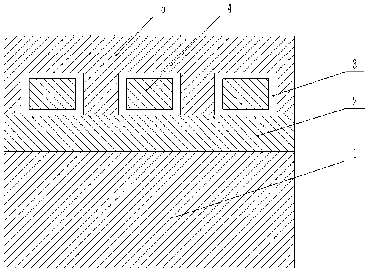
[0053] Such as figure 1 As shown, a BOX-shaped silicon nitride waveguide includes:

[0054] The first cladding layer 2 on the semiconductor substrate 1;

[0055] And the BOX silicon nitride waveguide 3 located on the first cladding layer 2; and the second cladding layer 4 located inside the BOX silicon nitride waveguide 3;

[0056] And a third cladding layer 5 located on the first cladding layer 2 and cladding the BOX silicon nitride waveguide 3;

[0057] The first coating layer 2, the second coating layer 4, and the third coating layer 5 include silicon dioxide;

[0058] The semiconductor substrate 1 is a silicon substrate;

[0059] The thickness of the first coating layer 2 is 3 μm; the thickness of the third coating layer 5 is 7 μm.

[0060] The manufacturing method of the BOX-shaped silicon nitride waveguide of this embodiment includes the following steps:

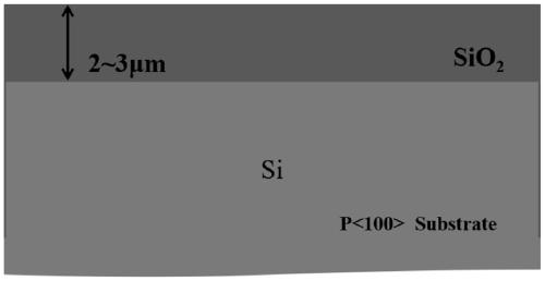
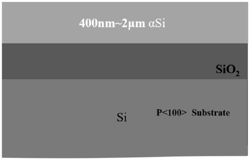
[0061] S1. Such as Figure 2-4 As shown, using thermal oxygen to grow 3μm thick SiO on a silicon substrate 2 Th...

Example Embodiment

[0077] Example 2

[0078] Such as figure 1 As shown, a BOX-shaped silicon nitride waveguide includes:

[0079] The first cladding layer 2 on the semiconductor substrate 1;

[0080] And the BOX silicon nitride waveguide 3 located on the first cladding layer 2; and the second cladding layer 4 located inside the BOX silicon nitride waveguide 3;

[0081] And a third cladding layer 5 located on the first cladding layer 2 and cladding the BOX silicon nitride waveguide 3;

[0082] The first coating layer 2, the second coating layer 4, and the third coating layer 5 include silicon dioxide;

[0083] The semiconductor substrate 1 is a silicon substrate;

[0084] The thickness of the first coating layer 2 is 2 μm; the thickness of the third coating layer 5 is 5 μm.

[0085] The manufacturing method of the BOX-shaped silicon nitride waveguide of this embodiment includes the following steps:

[0086] S1. Such as Figure 2-4 As shown, using thermal oxygen to grow 2μm thick SiO on a silicon substrate 2 Th...


PUM

PropertyMeasurementUnit
Thicknessaaaaaaaaaa
Thicknessaaaaaaaaaa
Thicknessaaaaaaaaaa

Abstract

The invention discloses a BOX-shaped silicon nitride waveguide and a preparation method thereof, and belongs to the technical field of optical materials, and the method comprises the steps: sequentially forming a first coating layer, a first sacrificial layer and a second sacrificial layer on a semiconductor substrate; etching the first sacrificial layer and the second sacrificial layer, and removing the second sacrificial layer to form a strip-shaped groove; growing a silicon nitride material, enabling one part of the silicon nitride material to grow in the strip-shaped groove, enabling one part of the silicon nitride material to cover the first sacrificial layer, and flattening the surface to form a BOX silicon nitride groove; growing a second coating layer, filling the BOX silicon nitride groove with a part of the second coating layer, covering the first sacrificial layer with a part of the second coating layer, and flattening the surface to form a smooth surface; growing a siliconnitride material and covering the smooth surface; etching the silicon nitride material outside the BOX silicon nitride groove to form a BOX silicon nitride waveguide, and etching the first sacrificiallayer; and growing a third coating layer on the first coating layer and the BOX silicon nitride waveguide, so that the problem that the perpendicularity of the dielectric material SiO2 is not high when the dielectric material SiO2 is directly etched by a traditional process is solved.

Description

Technical field [0001] The invention relates to the technical field of optical materials, in particular to a BOX-shaped silicon nitride waveguide and a preparation method thereof. Background technique [0002] Optical Waveguide (Optical Waveguide) is a dielectric device that guides light waves to propagate in it, also known as a dielectric optical waveguide. The dielectric waveguide is the basic structural unit of the integrated optical system and its components. The dielectric waveguide mainly plays the role of limiting, transmitting, and coupling light waves. Dielectric waveguides can be divided into four categories according to their cross-sectional shape: cylindrical waveguide (optical fiber), thin film (planar) waveguide, rectangular (strip) waveguide and ridge waveguide. Commonly used in integrated optics are thin film waveguides and rectangular waveguides (BOX waveguides). There are many types of materials used to form optical waveguides, and silicon nitride is currentl...

Claims


Application Information

Patent Timeline
IPC IPC(8): G02B6/122G02B6/13G02B6/136
CPCG02B6/122G02B6/13G02B6/136G02B2006/12035G02B2006/12166G02B2006/12176
Inventor 周章渝肖寒孙健代天军陈雨青彭晓珊王代强张青竹宁江华张子砚
Owner GUIYANG UNIV
Why Eureka
Try Eureka