Optical system structure for laser processing

An optical system and laser processing technology, applied in laser welding equipment, metal processing equipment, manufacturing tools, etc., can solve problems such as low production efficiency, increased workload of staff, and lack of versatility

Pending Publication Date: 2020-08-18
锡凡半导体无锡有限公司
View PDF1 Cites 3 Cited by
  • Summary
  • Abstract
  • Description
  • Claims
  • Application Information

AI Technical Summary

Problems solved by technology

[0003] 1. Waste of raw materials. Due to the mechanical structural elements of the mold, the corners of the PCB substrate cannot be punched, resulting in a relatively high material waste rate;
[0004] 2. The cost of the mold is high, and the formation of unused PCB boards requires different molds for stamping, which is not universal, and the mold is a consumable item that needs to be replaced regularly, and the cost is high;
[0005] 3. The mold processing takes a long time and the production efficiency is low. When making samples and small and medium-sized batches, the production takes a long time;
[0006] 4. The conventional process is prone to delamination and burrs, and will generate a lot of dust, which is not good for the environment;
[0007] 5. The conventional process is hard contact processing, which will generate stress when processing the PCB board and damage the substrate
[0010] The above-mentioned technical solution has the following defects: in the process of processing, since the position of the light spot departing from the galvanometer assembly is fixed, different positions on the PCB board need to be processed according to the processing requirements, and the PCB board needs to be moved in the XYZ axis direction, That is, the driving device is required to drive the installation tooling to move along the XYZ axis, which not only requires the use of driving parts, which increases the processing cost, but also needs to program the driving parts according to the processing requirements, which increases the workload of the staff

Method used


Image

  • Optical system structure for laser processing
  • Optical system structure for laser processing
  • Optical system structure for laser processing

Examples


Embodiment

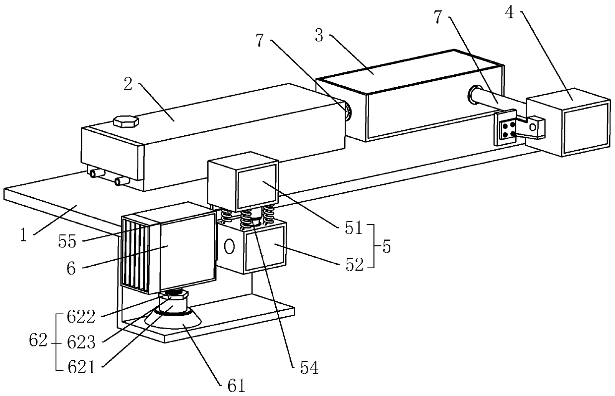
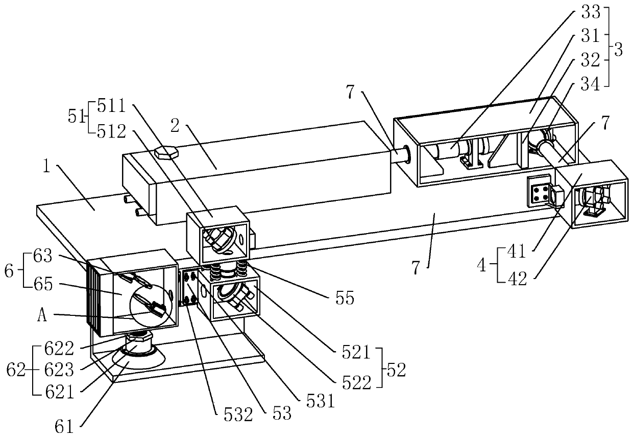
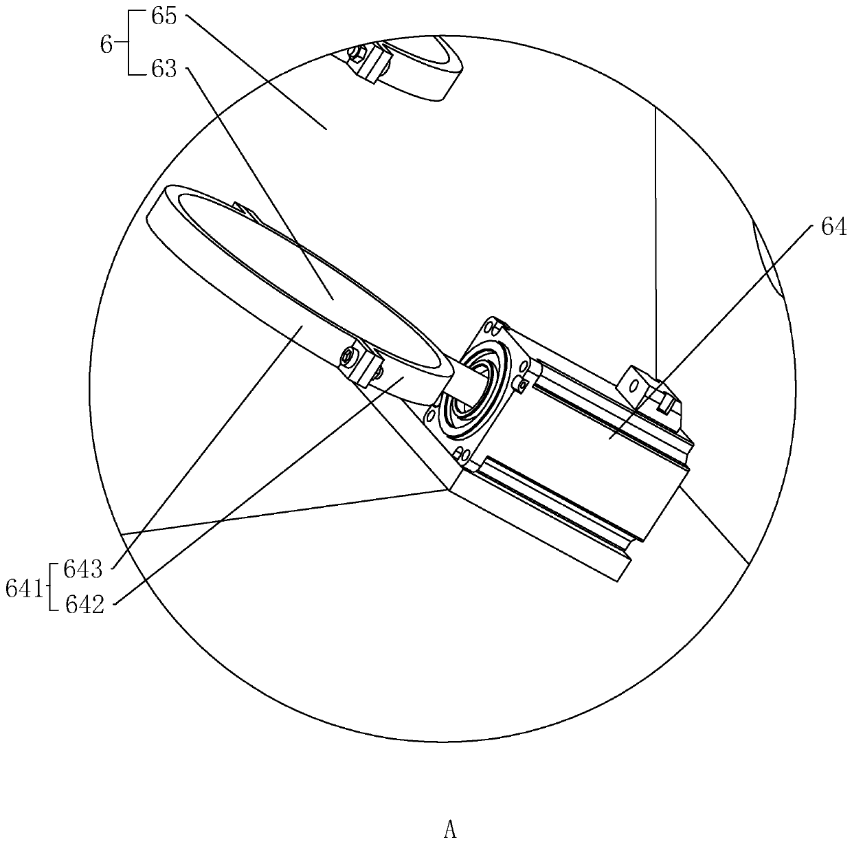
[0048] An optical system structure for laser processing, referring to figure 1 with figure 2 , including a frame 1, on which a laser 2, a beam expander assembly 3 connected to the exit end of the laser 2, a turning assembly 4 connected to the exit end of the beam expander assembly 3, and a turning assembly 4 connected to the exit The reflecting mechanism 5 at the end and the galvanometer assembly 6 connected to the output end of the reflecting mechanism 5, the laser 2 and the beam expander assembly 3, the beam expander assembly and the turning assembly 4 are all connected by a hollow shading rod 7.

[0049] refer to figure 1 with figure 2 , the laser is generated from the laser 2, emitted from the exit end of the laser 2, and enters the beam expander assembly 3 after passing through the light-shielding rod 7. The beam expander assembly 3 includes a box body 1 31 detachably connected to the frame 1 by bolts, The partition plate 32 fixedly connected in the box body one 31, ...


PUM


Abstract

The invention discloses an optical system structure for laser processing. The optical system structure for laser processing comprises a rack, wherein a laser, a beam expander assembly connected to theemergent end of the laser, a turning assembly connected to the emergent end of the beam expander assembly, a reflecting mechanism connected to the emergent end of the turning assembly and a galvanometer assembly connected to the emergent end of the reflecting mechanism are mounted on the rack, the laser and the beam expander assembly are connected through a hollow shading rod, the beam expander assembly and the turning assembly are connected through a hollow shading rod, the reflecting mechanism comprises a fixed end reflecting assembly and a movable end reflecting assembly connected below the fixed end reflecting assembly, and the fixed end reflecting assembly is mounted on the rack. The optical system structure for laser processing has the effect that the position of a light spot can berapidly adjusted, so that the light spot can move along the X axis, the Y axis and the Z axis.

Description

technical field [0001] The invention relates to the field of optical equipment, in particular to an optical system structure for laser processing. Background technique [0002] In the processing of PCB boards, die-cutting is often used at present. With the help of stamping equipment and molds, the entire PCB board is cut into the required shape. However, this method has many disadvantages: [0003] 1. Waste of raw materials. Due to the mechanical structural elements of the mold, the corners of the PCB substrate cannot be punched, resulting in a relatively high material waste rate; [0004] 2. The cost of the mold is high, and the formation of unused PCB boards requires different molds for stamping, which is not universal, and the mold is a consumable item that needs to be replaced regularly, and the cost is high; [0005] 3. The mold processing takes a long time and the production efficiency is low. When making samples and small and medium-sized batches, the production take...

Claims


Application Information

Patent Timeline
Patent Type & Authority Applications(China)
IPC IPC(8): B23K26/064B23K26/082
CPCB23K26/064B23K26/0643B23K26/082
Inventor 张斌刘伟罗豪
Owner 锡凡半导体无锡有限公司
Why Eureka
Try Eureka