Hard X-ray and photoelectron shielding composite material

A composite material and X-ray technology, which is applied in the field of hard X-ray and optoelectronic shielding composite materials, can solve the problems of poor shielding performance of hard X-rays, achieve poor shielding performance, excellent mechanical properties, and reduce the impact of optoelectronics on electronic equipment. the effect of

Active Publication Date: 2020-08-18
INST OF ELECTRONICS ENG CHINA ACAD OF ENG PHYSICS
View PDF4 Cites 2 Cited by
  • Summary
  • Abstract
  • Description
  • Claims
  • Application Information

AI Technical Summary

Problems solved by technology

[0005] The purpose of the present invention is to provide a hard X-ray and optoelectronic shielding composite material to solve the problem of poor shielding performance of existing hard X-ray shielding

Method used


Image

  • Hard X-ray and photoelectron shielding composite material
  • Hard X-ray and photoelectron shielding composite material
  • Hard X-ray and photoelectron shielding composite material

Examples


Embodiment 1

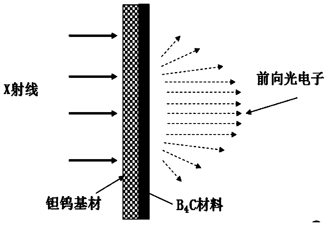
[0042] Such as figure 1 As shown, a kind of hard X-ray and optoelectronic shielding composite material comprises an X-ray shielding layer and a photoelectron shielding layer, the single side of the X-ray shielding layer is provided with an optoelectronic shielding layer, and the X-ray shielding layer is made of TaW alloy, The optoelectronic shielding layer adopts B 4 C is made, the thickness of the TaW alloy is 0.3mm, the B 4 The thickness of C is 50 μm, wherein, the mass fraction of TaW alloy W is 10%, and the mass fraction of Ta is 90%.

[0043] In this embodiment, the surface density of the TaW alloy is 0.5061g / cm 2 , the bulk density is 16.87g / cm 3 , the thermal conductivity is 47W / (m×K), and the thermal expansion coefficient is 5×10 -6 / K, tensile strength R m 830MPa, yield strength R p0.2 840MPa, the elongation A is 10%; the B 4 The thermal conductivity of C is 0.68~0.9W / (m×K), and the thermal expansion coefficient is 3.56×10 -6 / K(0~100℃)

[0044] The shield...

Embodiment 2

[0047] This embodiment is based on embodiment 1, and the difference with embodiment 1 is:

[0048] The thickness of the TaW alloy is 0.5mm, the B 4 C has a thickness of 100 μm.

[0049] In this embodiment, the surface density of the TaW alloy is 0.8435g / cm 2 , the bulk density is 16.87g / cm 3 , the thermal conductivity is 47W / (m×K), and the thermal expansion coefficient is 5×10 -6 / K, tensile strength R m 830MPa, yield strength R p0.2 840MPa, the elongation A is 10%; the B 4 The thermal conductivity of C is 0.68~0.9W / (m×K), and the thermal expansion coefficient is 3.56×10 -6 / K(0~100℃).

[0050] The cross-sectional morphology of the shielding composite material of this embodiment is as follows Figure 5 shown.

[0051] The shielding effect of the present embodiment:

[0052] 0.5mmTaW10 shields 94% of X-rays with 60KeV energy and 99% of 40KeV X-rays; 100μmB 4 C shields 91% of optoelectronics below 100KeV.

Embodiment 3

[0054] This embodiment is based on embodiment 1, and the difference with embodiment 1 is:

[0055] The thickness of the TaW alloy is 0.4mm, the B 4 C has a thickness of 80 μm.

[0056] In this embodiment, the surface density of the TaW alloy is 0.6748g / cm 2 , with a bulk density of 16.87g / cm 3 , the thermal conductivity is 47W / (m×K), and the thermal expansion coefficient is 5×10 -6 / K, tensile strength R m 830MPa, yield strength R p0.2 840MPa, the elongation A is 10%; the B 4 The thermal conductivity of C is 0.68~0.9W / (m×K), and the thermal expansion coefficient is 3.56×10 -6 / K(0~100℃)

[0057] The shielding effect of the present embodiment:

[0058] 0.4mmTaW10 shields 90% of X-rays with 60KeV energy and 99% of 40KeV X-rays; 80μmB 4 C shields 85% of optoelectronics below 100KeV.


PUM

PropertyMeasurementUnit
thicknessaaaaaaaaaa
thicknessaaaaaaaaaa
thicknessaaaaaaaaaa

Abstract

The invention discloses a hard X-ray and photoelectron shielding composite material, which comprises an X-ray shielding layer and a photoelectron shielding layer. The photoelectron shielding layer isarranged on two sides or one side of the X-ray shielding layer, the X-ray shielding layer is made of a high Z material, and the photoelectron shielding layer is made of a low Z material. The laminatedfunctional composite material composed of the high-Z material and the low-Z material can effectively shield X-rays and photoelectrons, the influence of the photoelectrons on electronic equipment is reduced, and the problem that an existing hard X-ray shielding material is poor in the shielding performance is solved.

Description

technical field [0001] The invention relates to the technical field of hard X-ray shielding, in particular to a hard X-ray and optoelectronic shielding composite material. Background technique [0002] The X-ray radiation environment will cause ionization damage to electronic devices and systems, which will cause the failure of electronic circuits and lead to the paralysis of the entire system. Therefore, X-ray shielding materials are required to shield X-rays to reduce ionization damage to electronic devices and systems. [0003] Existing X-ray shielding materials mainly use high atomic number metal materials (high Z metal materials), such as lead, tungsten-containing materials, etc. for hard X-ray shielding to reduce the total ionization dose on devices in the system. [0004] However, the existing X-ray shielding materials have poor shielding efficiency under a certain weight limit. At the same time, when X-rays pass through the metal shielding materials, a large number ...

Claims


Application Information

Patent Timeline
Patent Type & Authority Applications(China)
IPC IPC(8): G21F1/08G21F1/12C22C27/02
CPCG21F1/125G21F1/085C22C27/02
Inventor 朱小锋刘珉强赵洪超许献国周开明王艳
Owner INST OF ELECTRONICS ENG CHINA ACAD OF ENG PHYSICS
Why Eureka
Try Eureka