Photoelectric imaging sensor
A photoelectric imaging and sensor technology, applied in the field of photoelectric detection, can solve the problems of low quantum efficiency, large noise, and large volume, and achieve the effects of wide spectral response range, improved sensitivity, and reduced volume
- Summary
- Abstract
- Description
- Claims
- Application Information
AI Technical Summary
Problems solved by technology
Method used
Image
Examples
Embodiment Construction
[0026] Combine below Figure 1 to Figure 6 , the embodiment of the present invention and the specific operation process are described in detail, but the scope of protection of the present invention is not limited to the following examples.
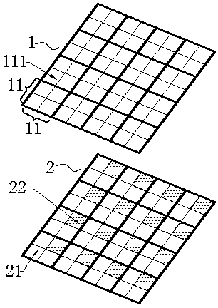
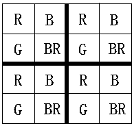
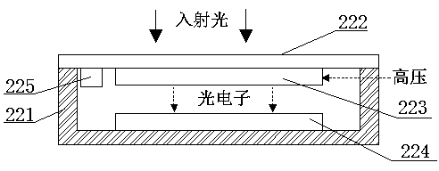
[0027] The invention discloses a photoelectric imaging sensor, comprising a filter layer 1 and an imaging unit 2, such as figure 1 As shown, the filter layer 1 is composed of several filter units 11, and each filter unit 11 includes four filter areas 111, and the four filter areas 111 allow red light, green light, blue light and broad-spectrum light to pass through respectively. , respectively named R, G, B, BR filter areas, such as figure 2 shown. The imaging unit 2 is used to receive the light passing through the filter layer 1 and perform imaging, including a visible light imaging unit 21 and a single photon imaging unit 22 ( figure 1 padding in ). The filter area that allows red light, green light and blue light to pass correspon...
PUM
 Abstract
Description
Claims
Application Information


