
Integrated IGBT packaging structure based on DBC layout
A packaging structure and layout technology, applied in the direction of semiconductor/solid-state device components, semiconductor devices, electrical components, etc., can solve the problems of reducing the IGBT working safety area, high installation process requirements, and large DC loop area, etc. The effect of expanding the working safety area, reducing the stray inductance and improving the power density
- Summary
- Abstract
- Description
- Claims
- Application Information
AI Technical Summary
Problems solved by technology
Method used
Image

Examples
Embodiment 1
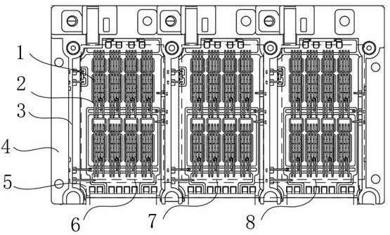
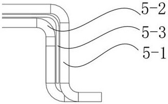
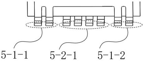
[0030] The integrated IGBT packaging structure based on a DBC layout includes a three-phase DBC structure, the outside of the three-phase DBC structure is fixed with a frame, the front of the three-phase DBC structure is welded with multiple chips, and the back of the three-phase DBC structure is directly welded on On the radiator, the chips in the three-phase DBC structure are connected to each other, and the DC terminals of the three-phase DBC structure are connected with laminated bus bars. The three-phase DBC of the present application is directly welded to the radiator. This process has one less substrate than the traditional process, which greatly reduces the thermal resistance and improves the power density; at the same time, this process is easy to realize automation and improves production efficiency. . A single DBC structure includes a ceramic insulating substrate 000. The front side of the ceramic insulating substrate 000 is provided with an upper bridge IGBT chip 00...
Embodiment 2
[0032] The integrated IGBT packaging structure based on a DBC layout includes a three-phase DBC structure, the outside of the three-phase DBC structure is fixed with a frame, the front of the three-phase DBC structure is welded with multiple chips, and the back of the three-phase DBC structure is directly Soldered on the heat sink, the chips in the three-phase DBC structure are connected to each other, and the DC terminals of the three-phase DBC structure are connected with laminated bus bars. The DBC structure includes a ceramic insulating substrate 000. The front side of the ceramic insulating substrate 000 is provided with an upper bridge IGBT chip 001, an upper bridge diode chip 002, a lower bridge IGBT chip 016, a lower bridge diode chip 017, an NTC temperature sensor 005 and multiple surfaces. Copper foil; the upper bridge IGBT chip 001 and the upper bridge diode chip 002 are connected by surface copper foil, the upper bridge diode chip 002 and the upper bridge IGBT chip 0...
PUM
 Abstract
Description
Claims
Application Information