

Satellite-borne data combiner multiplexer testing device and method
A technology for on-board data and testing devices, which is applied in electrical digital data processing, instruments, etc., can solve the problems of low transmission rate, many signal lines, unable to meet the data transmission requirements of on-board data multiplexers and acquisition equipment, etc. The effect of increasing the transfer rate
- Summary
- Abstract
- Description
- Claims
- Application Information
AI Technical Summary
Problems solved by technology
Method used
Image

Examples
Embodiment 1
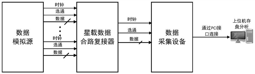
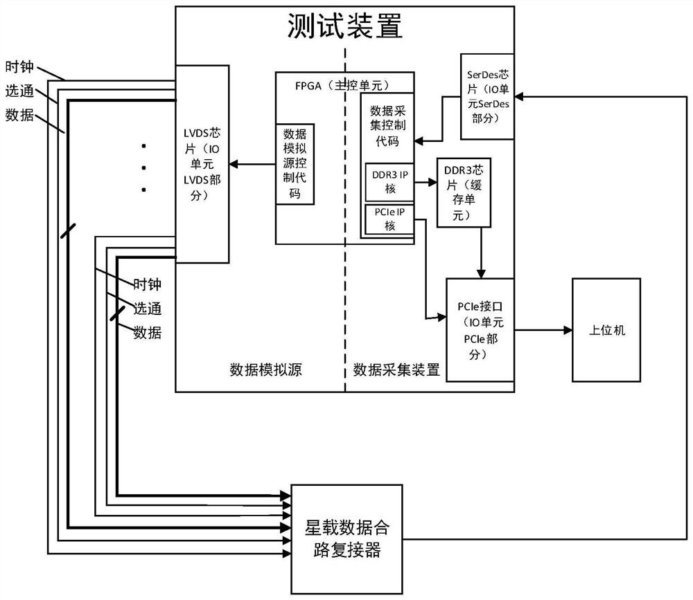
[0084] Such as image 3 As shown, Embodiment 1 of the present invention provides an on-board data multiplexer testing device. The device is used to test the spaceborne data combining multiplexer, and the device includes: an analog data generation module, a multiplexer data acquisition module and an analysis and comparison module set on the host computer.
[0085] The analog data generating module is divided functionally, including: an analog data generating unit and a data processing and sending unit.
[0086] The analog data generation module includes a main control part (FPGA module), a data simulation source control code part, an IO unit part (LVDS part) and a power supply unit. The FPGA module is connected to the LVDS chip;
[0087] The data simulation source control code part is used to generate data in the FPGA, and control the LVDS chip through the FPGA to send the data to the on-board data multiplexer;
[0088] The LVDS chip is used to convert the data generated by ...
Embodiment 2
[0114] Such as Figure 10 As shown, based on the above-mentioned system, Embodiment 2 of the present invention proposes a high-speed test method for an on-board data combiner multiplexer. The method specifically includes:
[0115] Step 1) After the device is powered on, the FPGA initializes and configures the LVDS chip, DDR3 chip, PCIe interface, and SerDes chip to make it work normally;
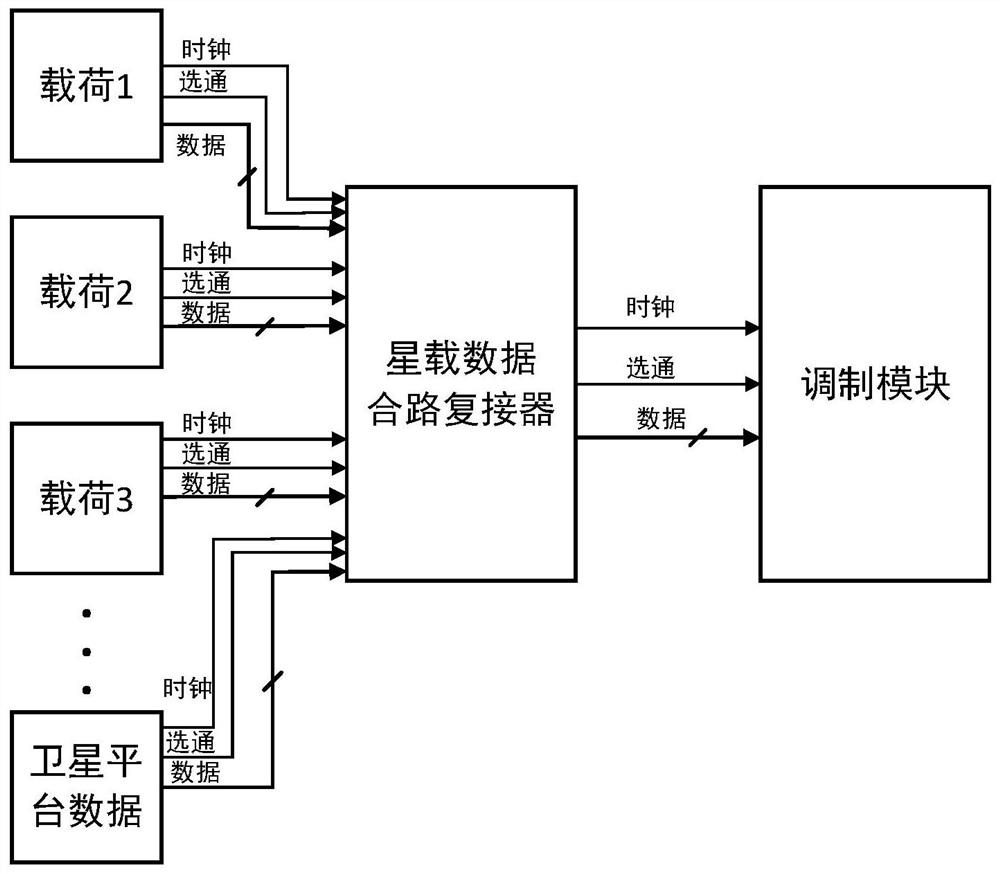
[0116] Step 2) The analog data generation unit of the analog data generation module, according to the test requirements and the specific conditions of the load, the simulated load generates a data source that meets the requirements, and after a fixed clock interval, each frame of image data is sequentially transmitted to the data processing and sending unit ;
[0117] Step 3) The data processing and sending unit of the analog data generation module converts each frame of image data received by controlling the LVDS chip from single-ended data to differential data, and sends them to the on-bo...
PUM
 Abstract
Description
Claims
Application Information