Semiconductor device and forming method thereof

A technology of semiconductors and devices, applied in the field of semiconductor devices and their formation, can solve problems affecting node contacts, abnormal morphology, etc.

Pending Publication Date: 2020-09-08
FUJIAN JINHUA INTEGRATED CIRCUIT CO LTD
View PDF0 Cites 0 Cited by
  • Summary
  • Abstract
  • Description
  • Claims
  • Application Information

AI Technical Summary

Problems solved by technology

[0005] The object of the present invention is to provide a semiconductor device to solve the abnormal shape of the node contact window formed on the edge of the memory area in the existing semiconductor device, thereby affecting the node contact portion filled in the node contact window

Method used


Image

  • Semiconductor device and forming method thereof
  • Semiconductor device and forming method thereof
  • Semiconductor device and forming method thereof

Examples


Embodiment 1

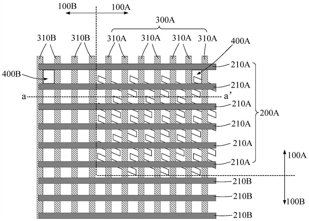
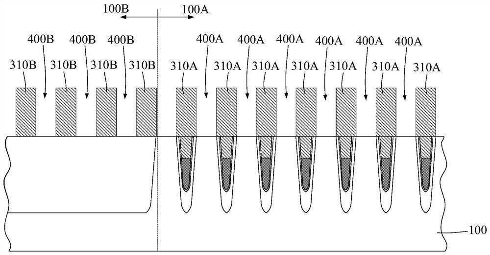
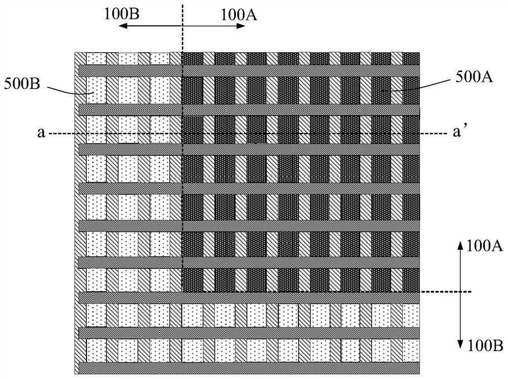
[0052] Figure 1a It is a top view of the semiconductor device in Embodiment 1 of the present invention that defines the node contact window and the auxiliary contact window, Figure 1b for Figure 1a The schematic cross-sectional view of the semiconductor device in the aa' direction shown in Embodiment 1 of the present invention, Figure 2aIt is a top view of the semiconductor device in Embodiment 1 of the present invention filled with node contacts and auxiliary filling columns, Figure 2b for Figure 2a Shown is a schematic cross-sectional view of the semiconductor device in the first embodiment of the present invention in the aa' direction.

[0053] specific reference Figure 1a ~ Figure 1b as well as Figure 2a ~ Figure 2b As shown, the semiconductor device includes a substrate 100 , and a set of bit lines 200A and a set of isolation lines 300A formed on the substrate 100 .

[0054] Wherein, a memory area 100A is defined on the substrate 100 , for example, a plurality...


PUM


Abstract

The invention provides a semiconductor device and a forming method thereof. A node contact window array is defined by using a bit line group and an isolation line group, an auxiliary line is further arranged, and an auxiliary contact window is defined at the periphery of the node contact window array by utilizing the auxiliary line, at this time, the auxiliary contact window is used, so that the arrangement density of the node contact windows in the edge area and the middle area in the node contact window array can be effectively balanced, the morphology precision of the node contact windows in the edge area is improved, and the morphology uniformity of the node contact windows in the edge area and the node contact windows in the middle area can be further improved.

Description

technical field [0001] The invention relates to the technical field of semiconductors, in particular to a semiconductor device and a forming method thereof. Background technique [0002] Memory, such as dynamic random access memory (Dynamic Random Access Memory, DRAM), which generally includes a storage capacitor and a storage transistor electrically connected to the storage capacitor, the storage capacitor is used to store charges representing stored information, and the storage transistor The storage capacitor can be electrically connected through a node contact. [0003] Currently, a method for preparing a node contact is, for example, using bit lines and isolation lines to define a node contact window, and then filling the node contact window with a conductive material to form a node contact. [0004] However, when the bit lines and isolation lines are prepared, the graphic morphology of the bit lines and isolation lines corresponding to the edge positions is easily def...

Claims


Application Information

Patent Timeline
Patent Type & Authority Applications(China)
IPC IPC(8): H01L27/108H01L23/528H01L21/8242
CPCH01L23/528H01L23/5283H10B12/30H10B12/485H10B12/482
Inventor 童宇诚赖惠先林昭维朱家仪
Owner FUJIAN JINHUA INTEGRATED CIRCUIT CO LTD
Why Eureka
Try Eureka