
Magnetic random access memory and forming method thereof

A random access memory and magnetic storage technology, applied in the field of memory, can solve problems affecting chip yield, magnetic tunnel junction damage, high density, etc.

Pending Publication Date: 2020-10-23
CHANGXIN MEMORY TECH INC
View PDF0 Cites 1 Cited by
  • Summary
  • Abstract
  • Description
  • Claims
  • Application Information

AI Technical Summary

Problems solved by technology

[0006] In the existing process technology nodes, the density of magnetic tunnel junctions per unit area of ​​MRAM is relatively high. During the process of etching to form magnetic tunnel junctions, it is easy to cause damage to the magnetic tunnel junctions and affect the chip yield.

Method used


Image

  • Magnetic random access memory and forming method thereof
  • Magnetic random access memory and forming method thereof
  • Magnetic random access memory and forming method thereof

Examples


Embodiment Construction

[0036] The specific implementation of the magnetic random access memory and its forming method provided by the present invention will be described in detail below in conjunction with the accompanying drawings.

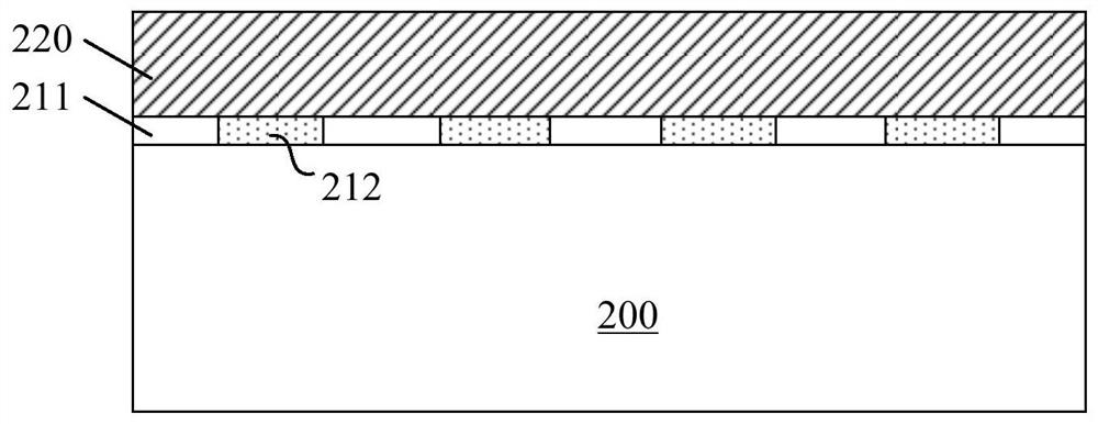
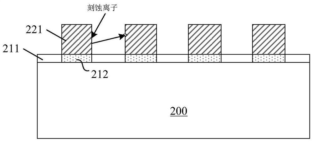
[0037] Please refer to Figure 2 to Figure 3 It is a structural schematic diagram of the formation process of the magnetic random access memory in a specific embodiment of the present invention.

[0038] Please refer to figure 2 , providing a substrate 200, forming a first metal layer 212 and a dielectric layer 211 on the surface of the substrate 200; forming a magnetic tunnel junction structure layer 220 on the deposition surface of the first metal layer 212 and the dielectric layer 211.

[0039] Please refer to image 3 , through the exposure and etching process, the magnetic tunnel junction structure layer 220 (please refer to figure 2 ) is patterned to form magnetic tunnel junction pillars 221 arranged in an array. Due to the higher requirements on the storag...


PUM


Abstract

The invention discloses a magnetic random access memory and a forming method thereof, and the magnetic random access memory comprises: a substrate, wherein a conductive contact pad is formed on the surface of the substrate; and a magnetic storage layer which is positioned on the surface of the substrate, wherein the magnetic storage layer comprises at least two sub-storage layers stacked on the surface of the substrate, the magnetic storage layer comprises a plurality of magnetic storage units which vertically penetrate through each sub-storage layer and are connected with the conductive contact pad, the plurality of magnetic storage units are arranged according to an array form of rhombus array units, each magnetic storage unit comprises a magnetic tunnel junction, and each sub-storage layer comprises at least one magnetic tunnel junction. The magnetic random access memory has relatively high performance.

Description

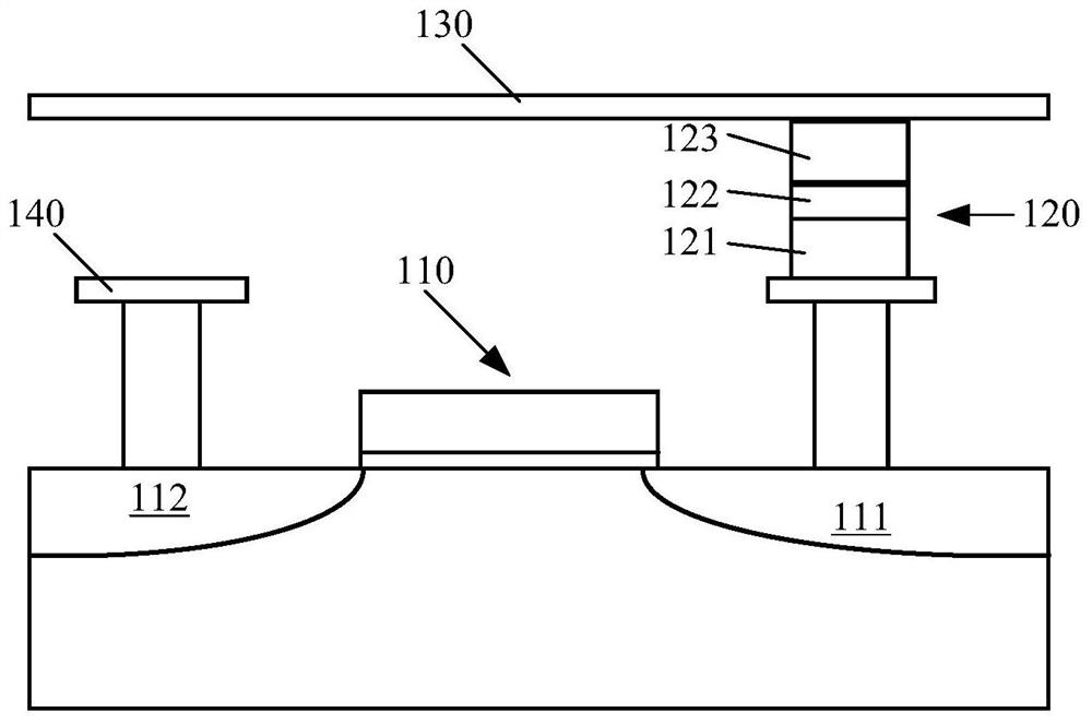
technical field [0001] The invention relates to the technical field of memory, in particular to a magnetic random access memory and a forming method thereof. Background technique [0002] Magnetic random access memory (MARM) is based on the integration of silicon-based complementary oxide semiconductor (CMOS) and magnetic tunnel junction (MTJ) technology. It is a non-volatile memory that has the high-speed read and write capabilities of static random access memory, and High integration of DRAM. [0003] Please refer to figure 1 , is a structural schematic diagram of an existing magnetic random access memory. [0004] The MRAM includes an access transistor 110 and a magnetic tunnel junction 120 , and the magnetic tunnel junction 120 includes a pinned layer 121 , a tunneling layer 122 and a free layer 123 . The drain 111 of the access transistor 110 is connected to the fixed layer 121 of the magnetic tunnel junction 120, and the free layer 123 of the magnetic tunnel junctio...

Claims


Application Information

Patent Timeline
Patent Type & Authority Applications(China)
IPC IPC(8): H01L27/22H01L43/08H01L43/12H10N50/01H10N50/10
CPCH10B61/20H10N50/10H10N50/01
Inventor 平尔萱朱一明
Owner CHANGXIN MEMORY TECH INC
Learn More