
Compound, thermal activation delayed fluorescence material and application thereof

A technology of thermally activated delayed and fluorescent materials, applied in the field of organic devices, can solve problems such as performance needs to be improved, and achieve the effects of improving luminous efficiency and working life, broadening the luminescent layer, and increasing the strength of the vibrator.

Active Publication Date: 2020-09-15
WUHAN TIANMA MICRO ELECTRONICS CO LTD
View PDF6 Cites 4 Cited by
  • Summary
  • Abstract
  • Description
  • Claims
  • Application Information

AI Technical Summary

Problems solved by technology

However, there are few TADF materials that have been discovered so far, and the performance needs to be improved. New TADF materials that can be used in OLED devices need to be developed urgently.

Method used


Image

  • Compound, thermal activation delayed fluorescence material and application thereof
  • Compound, thermal activation delayed fluorescence material and application thereof
  • Compound, thermal activation delayed fluorescence material and application thereof

Examples


preparation example 1

[0090] Synthesis of compound M3:

[0091]

[0092] (1) Add 5.60g (20mmol) of Compound A, 7.95g (20mmol) of Compound B, 8.94g (20mmol) of Compound C, 150mL of toluene, 13.81g (30mmol) of cesium carbonate, 0.23 g (0.2 mmol) of tetrakis(triphenylphosphine)palladium was reacted at 120° C. for 24 hours under a nitrogen atmosphere. Cool to room temperature, pour the reaction solution into 200mL ice water, extract three times with dichloromethane, combine the organic phases, spin into silica gel, and separate and purify by column chromatography (dichloromethane:n-hexane, v:v=1:1) to obtain Compound D.

[0093] 1 H NMR (400MHz, Chloroform) δ9.36(s,1H),9.08(s,1H),7.69(s,2H),7.58(s,1H),7.43(s,2H),7.36–7.29(m, 5H), 7.25(d, J=11.6Hz, 5H), 7.08(s, 2H), 7.00(s, 4H), 2.13(s, 6H).

[0094] 13 C NMR (100MHz, Chloroform) δ146.93(s), 140.83(s), 140.21(s), 134.42(s), 129.38–128.87(m), 127.54(s), 127.38–127.04(m), 125.65( s), 124.67(s), 122.99(s), 122.20(s), 121.16(s), 119.25(s), 95.28(s)...

preparation example 2

[0102] Synthesis of Compound M1

[0103]

[0104](1) Add 8.94g (20mmol) of Compound A, 3.98g (10mmol) of Compound B, 150mL of toluene, 13.81g (30mmol) of cesium carbonate, and tetrakis(triphenylphosphine) palladium in a 250mL three-necked flask. 0.23 g (0.2 mmol), and then reacted at 120° C. for 24 hours under a nitrogen atmosphere. Cool to room temperature, pour the reaction solution into 200mL ice water, extract three times with dichloromethane, combine the organic phases, spin into silica gel, and separate and purify by column chromatography (dichloromethane:n-hexane, v:v=1:1) to obtain Compound D.

[0105] 1 H NMR (400MHz, Chloroform) δ7.50–7.44(m,6H),7.32–7.24(m,8H),7.22–7.17(m,6H),7.14–7.07(m,10H),6.67(s,2H ),2.29(s,6H).

[0106] 13 C NMR (100MHz, Chloroform) δ146.34, 144.20, 137.71, 134.55, 134.13, 133.53, 130.17, 129.22, 127.64, 126.89, 125.87, 123.63, 122.29, 96.94, 14.03.

[0107] (2) In a 250ml three-neck flask, add 10.43g (10mmol) of substrate D (10mmol) a...

preparation example 3

[0114] Synthesis of compound M2

[0115]

[0116] (1) Add 9.22g (20mmol) of Compound A, 3.98g (10mmol) of Compound B, 150mL of toluene, 13.81g (30mmol) of cesium carbonate, and tetrakis(triphenylphosphine) palladium in a 250mL three-necked flask. 0.23 g (0.2 mmol), and then reacted at 120° C. for 24 hours under a nitrogen atmosphere. Cool to room temperature, pour the reaction solution into 200mL ice water, extract three times with dichloromethane, combine the organic phases, spin into silica gel, and separate and purify by column chromatography (dichloromethane:n-hexane, v:v=1:1) to obtain Compound D.

[0117] 1 H NMR (400MHz, Chloroform) δ7.52–7.46(m,4H),7.34–7.28(m,4H),7.15(dd,J=7.3,1.8Hz,6H),7.11(td,J=7.2,1.5 Hz,6H),7.07(td,J=7.3,1.8Hz,2H),6.78(dd,J=7.4,1.6Hz,4H),6.67(s,2H),2.29(s,6H).

[0118] 13 C NMR (100MHz, Chloroform) δ146.45, 139.72, 137.77, 134.55, 134.13, 133.40, 133.34, 130.17, 126.28, 126.22, 125.77, 123.92, 122.95, 120.19, 116.50, 946.034,

[0119] (2)...


PUM

PropertyMeasurementUnit
thicknessaaaaaaaaaa
thicknessaaaaaaaaaa
thicknessaaaaaaaaaa

Abstract

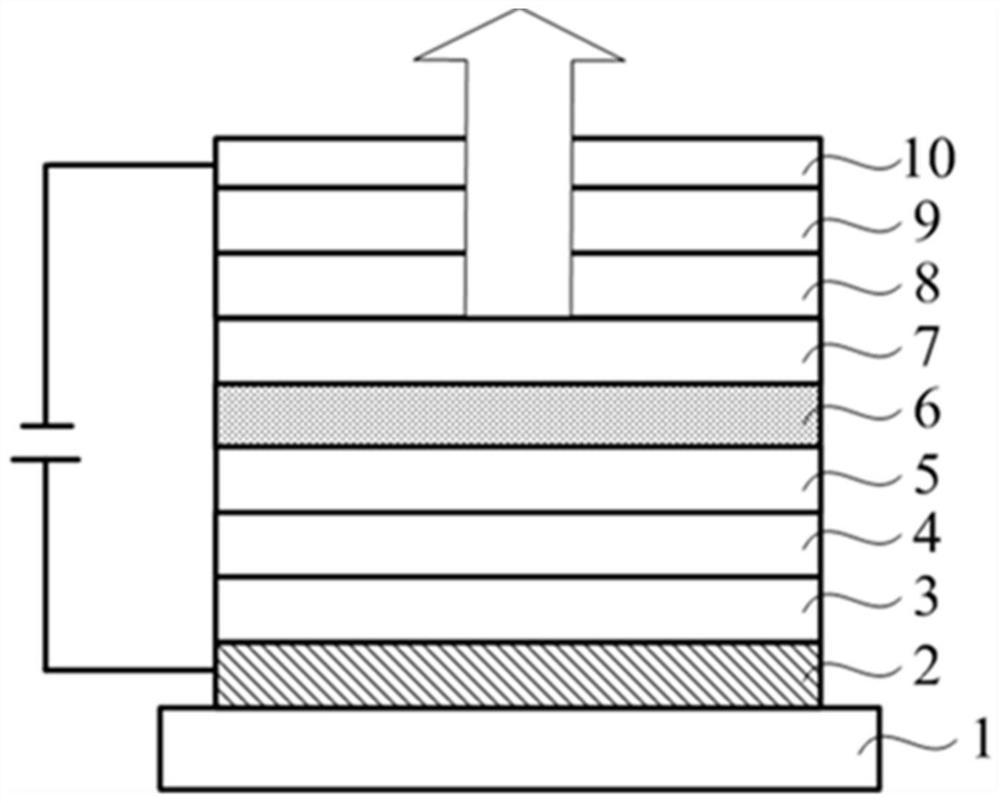
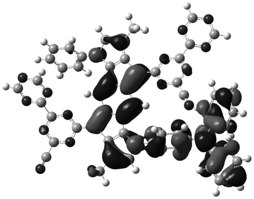
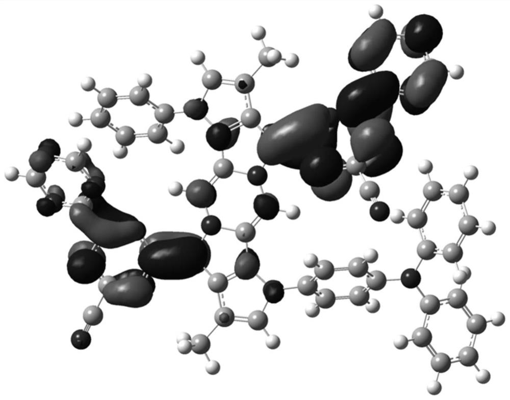
The invention provides a compound, a thermal activation delayed fluorescence material and application thereof, and particularly relates to a compound, a thermal activation delayed fluorescence material, a display panel and electronic equipment. The compound has structure as shown in formula I. The thermal activation delayed fluorescence material comprises any one or a combination of at least two of compounds; the display panel comprises an OLED device, the OLED device comprises an anode, a cathode and at least one organic layer located between the anode and the cathode, the organic layer comprises a light-emitting layer, and the light-emitting layer comprises the thermal activation delayed fluorescence material; the electronic equipment includes the display panel; the energy range delta Est between the lowest singlet state S1 and the lowest triplet state T1 of the compound is equal to ES1-ET1 and is less than or equal to 0.30 eV; the organic electroluminescent material has a thermal activation delayed fluorescence material luminescence mechanism, can be used in the field of organic photoelectric devices, reduces the driving voltage, improves the luminescence efficiency, prolongs the service life, and enables electronic equipment containing the organic electroluminescent material to have more excellent performances.

Description

technical field [0001] The invention belongs to the field of organic devices, and relates to a compound, a thermally activated delayed fluorescent material and an application thereof, in particular to a compound, a thermally activated delayed fluorescent material, a display panel and electronic equipment. Background technique [0002] In recent years, optoelectronic devices based on organic materials have become increasingly popular. The inherent flexibility of organic materials makes them very suitable for manufacturing on flexible substrates. They can design and produce beautiful and cool optoelectronic products according to requirements, and obtain incomparable advantages over inorganic materials. Examples of such organic optoelectronic devices include organic light emitting diodes (OLEDs), organic field effect transistors, organic photovoltaic cells, organic sensors, and the like. Among them, OLED is developing rapidly, and has achieved commercial success in the field o...

Claims


Application Information

Patent Timeline
Patent Type & Authority Applications(China)
IPC IPC(8): C07F5/02C09K11/06H01L51/50H01L51/54H01L27/32
CPCC07F5/02C09K11/06C09K2211/1007C09K2211/1014C09K2211/1059C09K2211/1044C09K2211/1085C09K2211/1033C09K2211/1088C09K2211/1074C09K2211/1037C09K2211/1029C09K2211/1092C09K2211/1011H10K59/00H10K85/623H10K85/615H10K85/622H10K85/624H10K85/653H10K85/631H10K85/626H10K85/654H10K85/655H10K85/657H10K85/6576H10K85/6572H10K85/6574H10K50/11Y02E10/549
Inventor 汪奎张正川
Owner WUHAN TIANMA MICRO ELECTRONICS CO LTD
Learn More