
Eureka
For R&D, Eureka makes reading and utilizing patents & technical documents easy.
Eureka AIR
Designed for self-driven R&D workflows. Generate viable solutions, solve complex R&D challenges, empower your innovation with AI.

Eureka Materials
Designed for material experts only. Revolutionize your material R&D, from search, analyze, to developing new materials.

TechResearch
Generate reliable direction feasibility study reports for your R&D in just a few steps.

TechSeek
Discover and master advanced knowledge NOW. Basics, ideas, possibilities, all at once.

TechMind
As an expert in R&D Theories, TechMind can generates customized viable solutions instantly.

TechRisk
Analyze your overall solution with one click, know your potential R&D risks in advance.

TechMonitor
Get weekly tech updates, stay abreast of the latest tech innovations and key insights.
Semiconductor device
A semiconductor and transistor technology, applied in the field of semiconductor devices, can solve the problems of engine mechanism damage, engine tempering, deflagration, etc., and achieve the effect of slow main current cut-off action and prevention of ignition action
- Summary
- Abstract
- Description
- Claims
- Application Information
AI Technical Summary
Problems solved by technology
Method used
Image

Examples
Embodiment approach 1
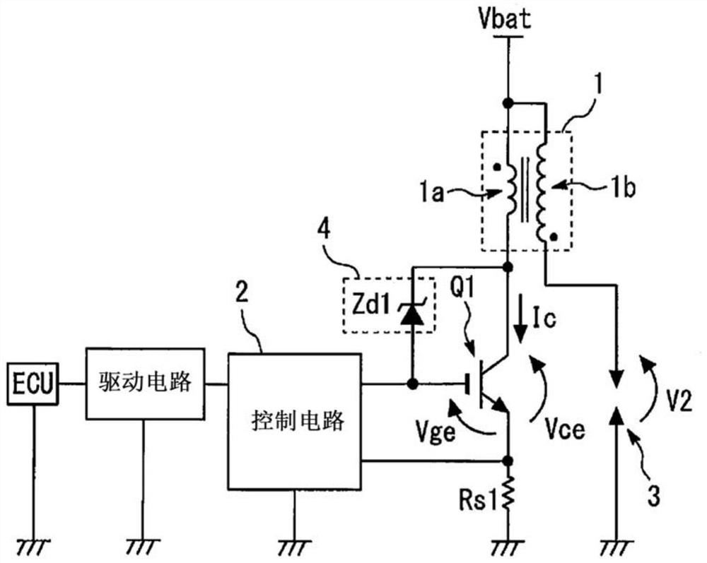
[0026] figure 1 It is a circuit diagram showing the semiconductor device according to Embodiment 1. This semiconductor device is used in an induction ignition type ignition system for an internal combustion engine such as an automobile engine. A power supply Vbat such as a battery is connected to one end of the primary side coil 1a and one end of the secondary side coil 1b of the ignition coil 1 as an L load. The power supply voltage Vbat is 14V. The gate of the insulated gate switching element Q1 is connected to the control circuit 2 , the collector is connected to the other end of the primary side coil 1 a , and the emitter is grounded via a resistor Rs1 . The threshold voltage Vth of the switching element Q1 is 2V. The resistance value of the resistor Rg1 is on the order of tens of kΩ. One end of the spark plug 3 is connected to the other end of the secondary side coil 1b, and the other end is grounded. The control circuit 2 controls the switching element Q1 in accorda...
Embodiment approach 2
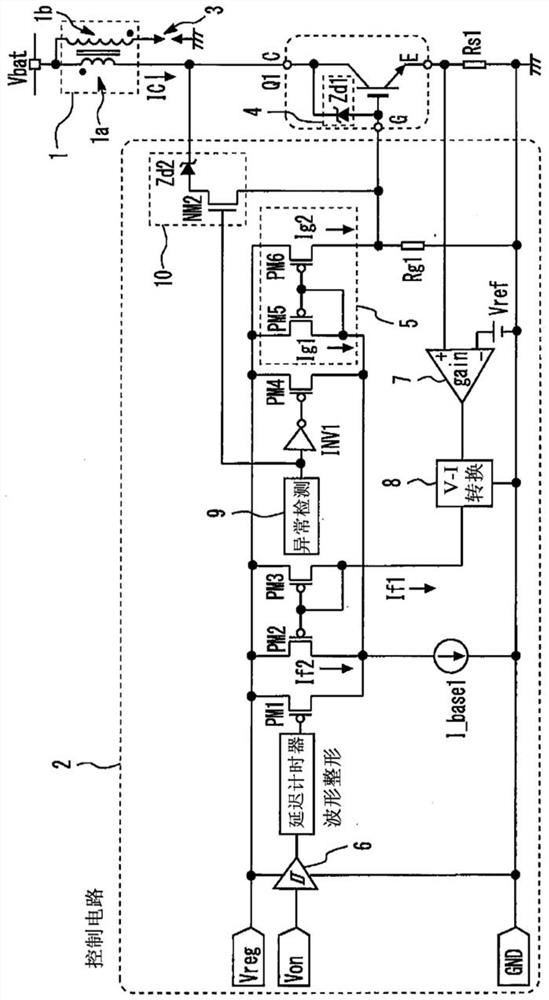
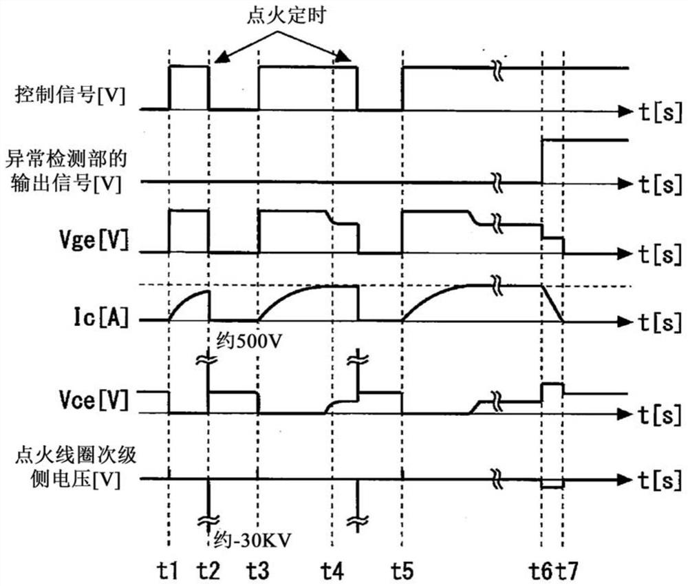
[0043] Figure 5 It is a diagram showing operation waveforms of the semiconductor device according to the second embodiment. In this embodiment, the gate capacitance of NM2 is set to be smaller than the gate capacitance of switching element Q1. As a result, when an operation abnormality is detected, NM2 is turned on before switching element Q1 is turned off, and thus a stable off operation of the second clamp circuit 10 can be realized. Other configurations and effects are the same as those in Embodiment 1.
Embodiment approach 3
[0045] Figure 6 It is a circuit diagram showing the semiconductor device according to Embodiment 3. In this embodiment, the delay timer 11 is connected between the gates of INV1 and PM4. The delay timer 11 delays a signal for controlling the drive unit 5 from the abnormality detection unit 9 . As a result, when abnormal operation is detected, NM2 is turned on before switching element Q1 is turned off, and a stable off operation of the second clamp circuit 10 can be realized. Other configurations and effects are the same as those in Embodiment 1.
PUM
 Abstract
Description
Claims
Application Information
 - R&D Engineer
- R&D Manager
- IP Professional
- Industry Leading Data Capabilities
- Powerful AI technology
- Patent DNA Extraction
Browse by: Latest US Patents, China's latest patents, Technical Efficacy Thesaurus, Application Domain, Technology Topic, Popular Technical Reports.
© 2024 PatSnap. All rights reserved.Legal|Privacy policy|Modern Slavery Act Transparency Statement|Sitemap|About US| Contact US: help@patsnap.com