ESD protection circuit and electronic device

An ESD protection and circuit technology, applied in emergency protection circuit devices, electric solid-state devices, circuits, etc., can solve problems such as difficult performance improvement, and achieve the effect of improving heat dissipation uniformity and good heat dissipation

Active Publication Date: 2020-09-22
SEMICON MFG INT (SHANGHAI) CORP +1
View PDF10 Cites 3 Cited by
  • Summary
  • Abstract
  • Description
  • Claims
  • Application Information

AI Technical Summary

Problems solved by technology

[0004] However, there are limitations in the circuit structure of existing ESD protection circuits, making it difficult to improve the performance

Method used


Image

  • ESD protection circuit and electronic device
  • ESD protection circuit and electronic device
  • ESD protection circuit and electronic device

Examples


Embodiment Construction

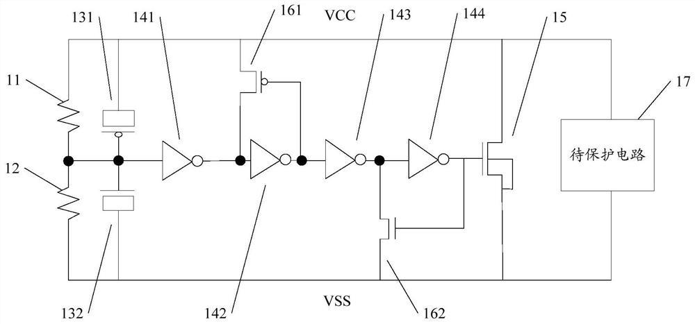
[0031] In the prior art, when clamping transistors are used to form an ESD protection circuit, the active circuit of the N-type clamping transistor is often driven by the gate, and the clamping transistor is coupled between the power supply terminal and the ground terminal. Core devices are protected.

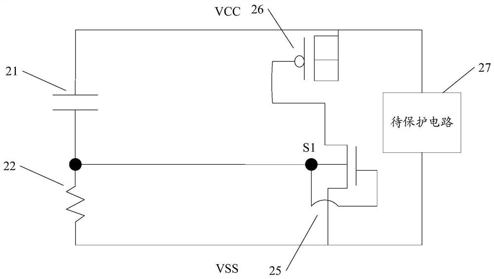
[0032] refer to figure 1 , figure 1 It is a schematic circuit structure diagram of an ESD protection circuit in the prior art. The ESD protection circuit can be used to protect the circuit 17 to be protected, and can also include:

[0033] power terminal;

[0034] ground terminal;

[0035] The discharge path includes a clamping transistor 15, the clamping transistor 15 is an N-type transistor, and the source of the clamping transistor 15 is connected to the power supply terminal, and the drain of the clamping transistor 15 is connected to the The ground terminal, and the substrate terminal of the clamp transistor 15 is connected to the source;

[0036] a first resistor 11...


PUM


Abstract

The invention discloses an ESD protection circuit and an electronic device. The ESD protection circuit comprises a power supply end; a ground end; a discharge circuit which comprises a clamping transistor and an MOS transistor which are connected in series, wherein the clamping transistor and the MOS transistor are integrated on the same semiconductor substrate and are different in type, and the source electrode and the drain electrode of the clamping transistor are electrically connected with the substrate end and are connected to the power supply end; the grid electrode of the MOS transistoris electrically connected with the substrate end; the first electrode of the MOS transistor is electrically connected with the grid electrode of the clamping transistor, and the second electrode of the MOS transistor is connected with the grounding end; when ESD occurs, the MOS transistor is turned on, and parasitic current between the substrate end of the clamping transistor and the second electrode is formed. According to the scheme of the invention, the leakage current generated by the discharge path can be better prevented, and the quality of the core device is prevented from being influenced.

Description

technical field [0001] The invention relates to the technical field of semiconductors, in particular to an ESD protection circuit and an electronic device. Background technique [0002] With the rapid development of the semiconductor manufacturing process, devices with ultra-thin gate oxide layers and thin dielectrics are increasing, and the electrostatic discharge (Electro-Static Discharge, ESD) problem has gradually become one of the main factors of chip failure. Taking Fin Field Effect Transistor (FinFET) as an example, in the face of the high leakage problem of multiple Fin structures, the ESD protection circuit inside the chip is indispensable. [0003] In the prior art, there already exists a protection scheme that adopts a clamp circuit (Clamp Circuit) including a clamp transistor (Clamp Transistor) as an ESD protection circuit. Specifically, the ESD protection circuit drives an N-type An active circuit of a clamping transistor, and the clamping transistor is coupled...

Claims


Application Information

Patent Timeline
Patent Type & Authority Applications(China)
IPC IPC(8): H02H9/04
CPCH02H9/046H01L27/0262H01L27/0285H01L27/092H01L27/0277H01L27/0288H03K17/08104
Inventor 陈光陈捷
Owner SEMICON MFG INT (SHANGHAI) CORP
Why Eureka
Try Eureka