

Method for calibrating silicon nanowire sensor by using cursor
A silicon nanowire and sensor technology, applied in the field of sensors, can solve problems such as inability to perform accurate quantitative testing, silicon nanowire size deviation, affecting device consistency, etc., and achieve the effects of stable test results, low cost, and convenient testing.
- Summary
- Abstract
- Description
- Claims
- Application Information
AI Technical Summary
Problems solved by technology
Method used
Image

Examples
Embodiment Construction
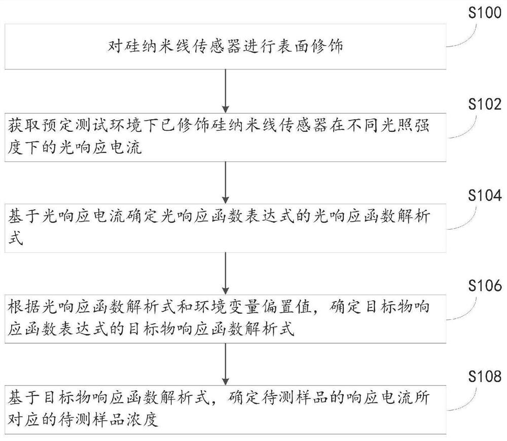
[0046] In order to make the purpose, technical solutions and advantages of the embodiments of the present invention clearer, the technical solutions in the embodiments of the present invention will be clearly and completely described below in conjunction with the drawings in the embodiments of the present invention. Obviously, the described embodiments It is a part of embodiments of the present invention, but not all embodiments. Based on the embodiments of the present invention, all other embodiments obtained by those skilled in the art without making creative efforts belong to the protection scope of the present invention. In order to solve the problems in the prior art, the present invention provides a method for using a cursor to determine a silicon nanowire sensor, such as figure 1 As shown, the method includes:
[0047] S100, modifying the surface of the silicon nanowire sensor;
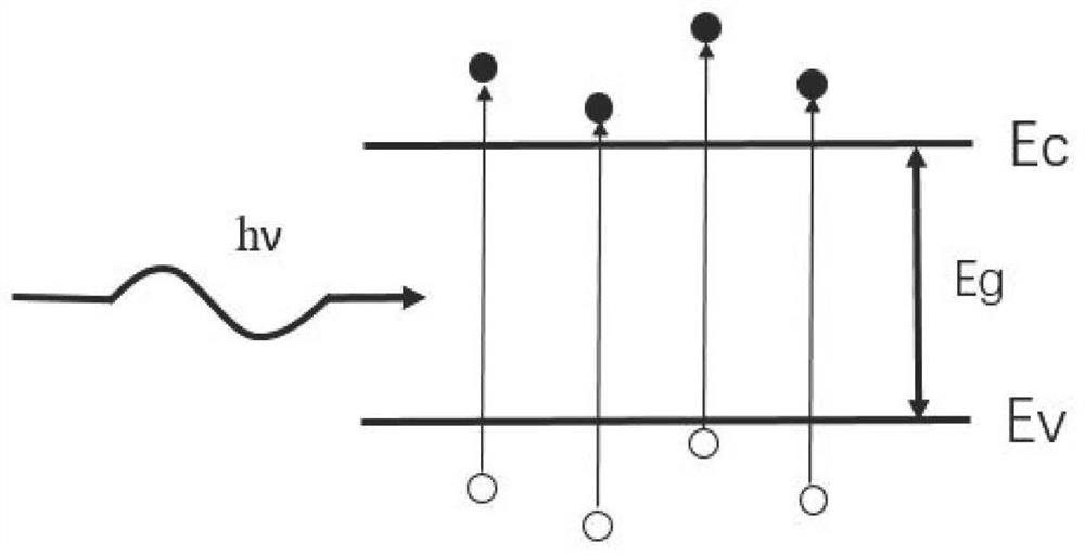
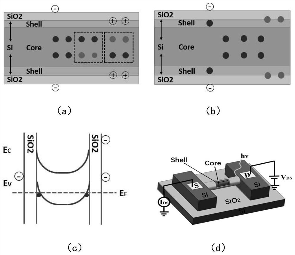
[0048] Specifically, the present invention intends to use the photoresponse of the silico...
PUM
 Abstract
Description
Claims
Application Information