
Method and structure for bonding light emitting diode and substrate

A technology of light-emitting diodes and substrates, which is applied to electrical components, electrical solid devices, circuits, etc., and can solve problems such as difficulties in the manufacturing process, increased costs, and inability to completely bond N-type contact pads and P-type contact pads.

Inactive Publication Date: 2020-09-29
PRILIT OPTRONICS INC
View PDF4 Cites 0 Cited by
  • Summary
  • Abstract
  • Description
  • Claims
  • Application Information

AI Technical Summary

Problems solved by technology

Therefore, when flip-chip bonding the LED to the glass substrate, the balance is usually not reached, so that the N-type contact pad and the P-type contact pad cannot be completely bonded to the glass substrate.
[0005] In order to overcome the above shortcomings, the traditional method is to thicken the N-type contact pad, but it requires additional manufacturing process steps, uses more materials, and causes difficulties in the manufacturing process and increases costs.

Method used


Image

  • Method and structure for bonding light emitting diode and substrate
  • Method and structure for bonding light emitting diode and substrate
  • Method and structure for bonding light emitting diode and substrate

Examples


Embodiment Construction

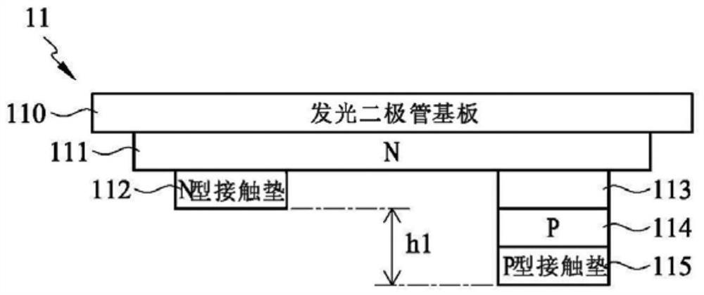
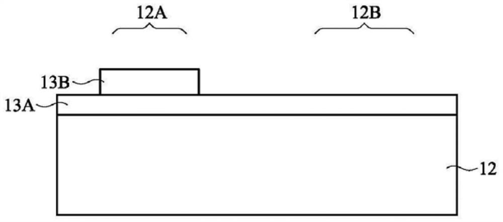
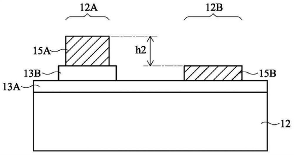
[0021] Figure 1A to Figure 1D The cross-sectional view of FIG. 1 shows the method for bonding the LED 11 and the substrate 12 according to the first embodiment of the present invention.

[0022] refer to Figure 1A , providing (inverted) light emitting diodes 11 disposed on the bottom surface of a light emitting diode substrate 110 (such as sapphire, gallium arsenide (GaAs), silicon carbide (SC) or other suitable materials). Wherein, the LED 11 may include an N-type layer 111 disposed on the bottom surface of the LED substrate 110 ; and an N-type contact pad 112 disposed on the bottom surface of the N-type layer 111 . The LED 11 may include a potential well 113 , such as a multiple quantum well (MQW), disposed on the bottom surface of the N-type layer 111 . The LED 11 may include a P-type layer 114 disposed on the bottom surface of the potential energy well 113 ; and a P-type contact pad 115 disposed on the bottom surface of the P-type layer 114 . A first height difference ...


PUM


Abstract

A method of bonding a light emitting diode and a substrate includes the steps: providing the light emitting diode disposed on the bottom surface of the light emitting diode substrate; comprehensivelyforming a first insulating layer on the substrate; forming a second insulating layer on the first insulating layer and located in the first region, wherein the second insulating layer corresponds to an N-type contact pad of the light emitting diode; forming a first conductor layer on the second insulating layer and located in the first region; forming a second conductor layer on the first insulating layer and located in the second region, wherein the second conductor layer corresponds to a P-type contact pad of the light emitting diode; and bonding the light emitting diode to the substrate, wherein the N-type contact pad is connected to the first conductor layer and located in the first region, and the P-type contact pad is connected to the second conductor layer and located in the secondregion.

Description

technical field [0001] The invention relates to a light-emitting diode, in particular to a method for bonding a light-emitting diode and a substrate. Background technique [0002] A light emitting diode is a semiconductor light source with two electrodes. Light-emitting diodes include p-n junction diodes that emit light by combining electrons and holes when activated. [0003] Generally, flip chip technology is used to bond the LED and the glass substrate. Flip the LED over so that it is face down, then align the contact pads of the LED with the corresponding contact pads of the glass substrate to complete the bonding. [0004] However, the top surface of the N-type contact pad and the top surface of the P-type contact pad are usually not located at the same level. For example, the P-type contact pad is about 1-3 microns higher than the N-type contact pad. Therefore, when the light-emitting diode is flip-chip bonded to the glass substrate, a balance is usually not achiev...

Claims


Application Information

Patent Timeline
IPC IPC(8): H01L25/075H01L33/00H01L33/20
CPCH01L25/0753H01L33/005H01L33/20
Inventor 吴炳昇李杏樱吴昭文
Owner PRILIT OPTRONICS INC
Learn More