Manufacturing method of self-aligned contact hole and manufacturing method of semiconductor device

A technology of self-aligned contact holes and manufacturing methods, which is applied in semiconductor/solid-state device manufacturing, semiconductor devices, semiconductor/solid-state device components, etc., can solve problems such as short circuit, uncontrollable contact hole shape, device failure, etc., to achieve The effect of large process window, improved product competitiveness, and small chip area

Active Publication Date: 2020-10-02
WUHAN XINXIN SEMICON MFG CO LTD
View PDF9 Cites 3 Cited by
  • Summary
  • Abstract
  • Description
  • Claims
  • Application Information

AI Technical Summary

Problems solved by technology

[0008] However, with the continuous shrinking of process nodes, the key physical dimensions and film thickness are also constantly evolving, and further shrinking of the distance S between the contact hole and the polysilicon gate is also imminent, resulting in the etching stop layer 105 becoming more and more Thin
However, when the etch stop layer 105 is too thin to serve as a contact hole etch stop layer, the contact hole morphology becomes uncontrollable, such as image 3 As shown, the etch stop layer 105 is too thin, and the etch selectivity ratio of the interlayer dielectric layer 106 to the etch stop layer 105 is only between 5 and 50, which is not high enough, which will cause the contact hole to be etched. The etch stop layer 105 on the surface of the sidewall 104 and the source-drain region 101 will also be etched away, and the exposed sidewall 104, the sidewall of the interlayer dielectric layer 106 and the source-drain region 101 will be etched, forming a contact hole in the shape of appearance deviated figure 2 As shown in the ideal shape, the formed contact plug 107b is electrically contacted with the polysilicon gate 103 and the source-drain region 101, and the polysilicon gate 103 and the source-drain region 101 are short-circuited, causing device failure

Method used


Image

  • Manufacturing method of self-aligned contact hole and manufacturing method of semiconductor device
  • Manufacturing method of self-aligned contact hole and manufacturing method of semiconductor device
  • Manufacturing method of self-aligned contact hole and manufacturing method of semiconductor device

Examples


Embodiment Construction

[0063] The technical solutions proposed by the present invention will be described in further detail below in conjunction with the accompanying drawings and specific embodiments. The advantages and features of the present invention will become clearer from the following description. It should be noted that all the drawings are in a very simplified form and use imprecise scales, and are only used to facilitate and clearly assist the purpose of illustrating the embodiments of the present invention. In this article, the meaning of "and / or" is to choose one or both.

[0064] Please refer to Figure 4 , an embodiment of the present invention provides a method for manufacturing a self-aligned contact hole, comprising the following steps:

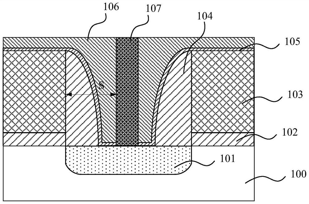
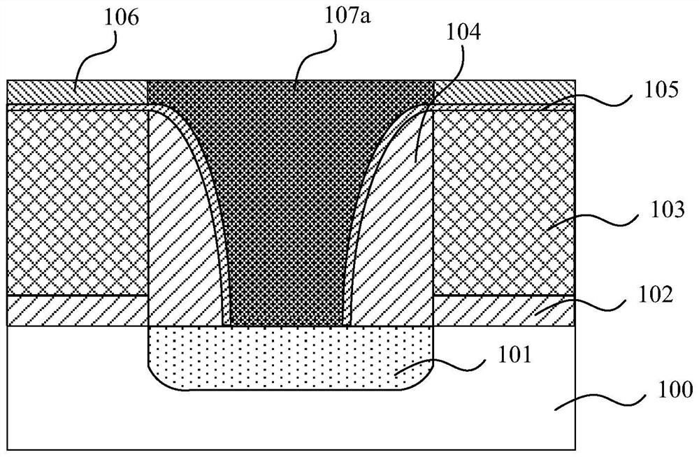
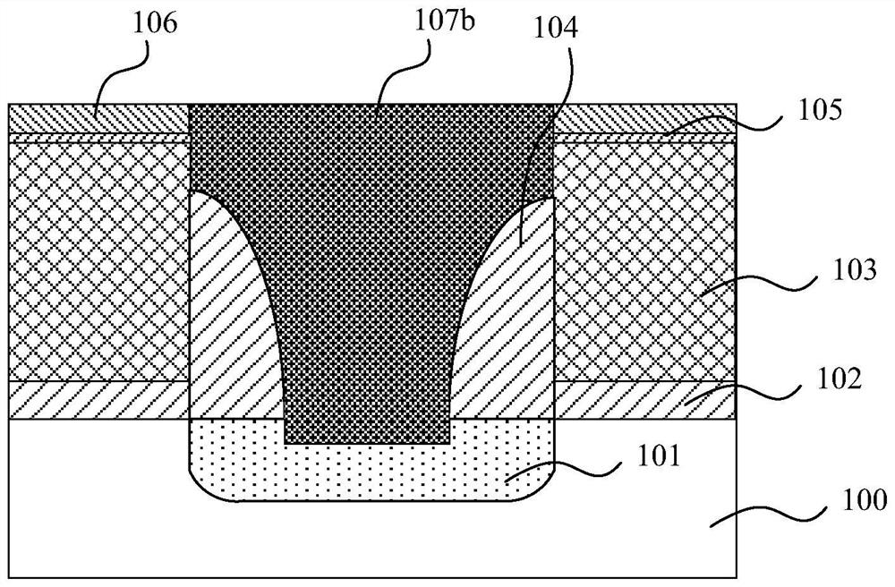
[0065] S1, providing a substrate, on which a plurality of gate stack structures and sidewalls located on both sides of each gate stack structure are formed, and trenches are formed between sidewalls on opposite sides of adjacent gate stack struc...


PUM


Abstract

The invention provides a manufacturing method of a self-aligned contact hole and a manufacturing method of a semiconductor device. The method comprises the following steps of filling a sacrificial material layer in a trench between adjacent gate stack structure, removing the sacrificial material layer outside the region where the contact hole is to be formed, forming an opening in the sacrificialmaterial layer, filling the opening with an insulating dielectric layer, removing the sacrificial material layer through a selective etching process, so as to avoid etching loss to the insulating dielectric layer around the sacrificial material layer, the side wall and the bottom etching stop layer or the liner oxide layer in the process of removing the sacrificial material layer. The morphology of the formed self-aligned contact hole can be accurately controlled, further reduction of the distance between the contact hole and the gate is facilitated, and the size of the chip is reduced.

Description

technical field [0001] The invention relates to the technical field of manufacturing semiconductor devices, in particular to a method for manufacturing self-aligned contact holes and a method for manufacturing semiconductor devices. Background technique [0002] In pursuit of lower chip manufacturing costs, it is common practice to minimize chip area without affecting chip performance. Among the many factors affecting the chip area, the distance between the contact hole and the polysilicon gate is a link that cannot be ignored. [0003] Please refer to figure 1 As shown, in the traditional chip manufacturing process, the common practice is: first, after forming the gate dielectric layer 102 and the polysilicon gate 103 on the substrate 100, make a spacer (spacer) 104 on the sidewall of the polysilicon gate 103, and further A source-drain region 101 is formed in the substrate 100 by a source-drain ion implantation process; then, an etching stop layer (Etching StopLayer, ESL...

Claims


Application Information

Patent Timeline
IPC IPC(8): H01L21/768H01L23/48H01L21/48
CPCH01L21/4814H01L21/76805H01L21/76816H01L21/76897H01L23/481H01L29/66477
Inventor 杨道虹周俊孙鹏
Owner WUHAN XINXIN SEMICON MFG CO LTD
Why Eureka
Try Eureka