Avalanche photodiode with three-mesa structure and manufacturing method thereof

A technology of avalanche optoelectronics and mesa structure, which is applied in the direction of circuits, electrical components, semiconductor devices, etc., can solve problems such as edge breakdown, lower reliability, and affect the normal operation of devices, so as to reduce parasitic capacitance, improve reliability, and suppress The effect of the fringe electric field breakdown phenomenon

Pending Publication Date: 2020-10-02
FUJIAN Z K LITECORE LTD
View PDF0 Cites 4 Cited by
  • Summary
  • Abstract
  • Description
  • Claims
  • Application Information

AI Technical Summary

Problems solved by technology

[0002] InP-based avalanche photodiodes have the advantages of high sensitivity and high responsivity. As the core part of optical receivers, they are widely used in optical communication systems. When manufacturing avalanche photodiodes with traditional planar structures, the size of the photosensitive surface of the device is determined by the Zn diffusion. The window is determined, and the curvature effect of the diffusion window makes the electric field intensity at the edge higher than the central area of ​​the photosensitive surface, which easily causes edge breakdown at the edge of the diffusion window, affects the normal operation of the device, and reduces reliability

Method used


Image

  • Avalanche photodiode with three-mesa structure and manufacturing method thereof
  • Avalanche photodiode with three-mesa structure and manufacturing method thereof
  • Avalanche photodiode with three-mesa structure and manufacturing method thereof

Examples


Embodiment Construction

[0037] The present invention will be further described in detail below in conjunction with the accompanying drawings and specific embodiments.

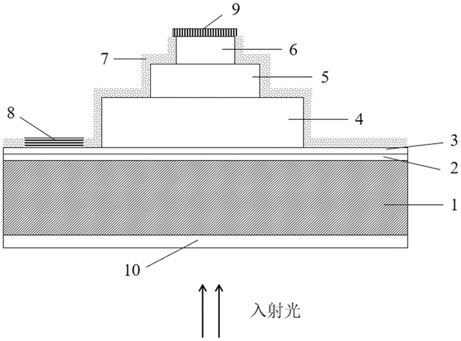
[0038] Such as figure 1 As shown, the present invention provides an avalanche photodiode with a three-mesa structure, comprising a Fe-InP substrate 1, an InP buffer layer 2, a P-type InGaAsP contact layer 3, a third mesa 4, a second Mesa 5 and first mesa 6. A P electrode 8 and an N electrode 9 are arranged above the P-type InGaAsP contact layer and the N-type InGaAs contact layer respectively. SiO is provided on the top and sidewalls of the three-mesa structure 2 Passivation layer 7. An anti-reflection film 10 is provided on the back of the Fe-InP substrate. When the avalanche photodiode is working, light is incident from the back of the substrate.

[0039] Since there is a large band step between the light-absorbing layer InGaAs and InP, the discontinuity of the energy band will generate a potential barrier, hinder the movement o...


PUM


Abstract

The invention relates to an avalanche photodiode with a three-mesa structure and a manufacturing method thereof. The avalanche photodiode comprises a Fe-InP substrate, an InP buffer layer, a P-type InGaAsP contact layer, a third mesa, a second mesa and a first mesa which are arranged from bottom to top, wherein the third mesa comprises a P-type InP corrosion cut-off layer, a P-type InGaAsP gradient layer, a P-type InGaAs light absorption layer, an i-type InGaAs light absorption layer, a P-type AlGaInAs gradient layer, a P-type InP charge layer and an i-type InAlAs multiplication layer which are arranged from bottom to top; the second mesa comprises an N-type InP charge layer and an N-type InP edge electric field buffer layer which are arranged from bottom to top; the first mesa comprises an N-type InGaAs contact layer. According to the avalanche photodiode and the manufacturing method thereof, the reliability, high speed and high bandwidth performance of the avalanche photodiode can beimproved.

Description

technical field [0001] The invention relates to the technical field of photodiodes, in particular to an avalanche photodiode with a three-mesa structure and a manufacturing method thereof. Background technique [0002] InP-based avalanche photodiodes have the advantages of high sensitivity and high responsivity. As the core part of optical receivers, they are widely used in optical communication systems. When manufacturing avalanche photodiodes with traditional planar structures, the size of the photosensitive surface of the device is determined by the Zn diffusion. The window is determined, and the curvature effect of the diffusion window makes the electric field intensity at the edge higher than the central area of ​​the photosensitive surface, which is easy to cause edge breakdown at the edge of the diffusion window, affecting the normal operation of the device and reducing reliability. [0003] Existing methods to suppress edge breakdown generally adopt diffusion or ion ...

Claims


Application Information

Patent Timeline
Patent Type & Authority Applications(China)
IPC IPC(8): H01L31/107H01L31/0236H01L31/0352H01L31/18
CPCH01L31/02366H01L31/035281H01L31/107H01L31/18
Inventor 叶旺陈景源李欣
Owner FUJIAN Z K LITECORE LTD
Why Eureka
Try Eureka