Nanosheet field effect transistor and preparation method thereof

A field effect transistor and nanosheet technology, applied in the field of nanosheet field effect transistors and their preparation, can solve problems such as nanosheet damage, and achieve the effects of increasing protection, reducing gate delay effect and increasing stability

Pending Publication Date: 2020-10-09
SIEN QINGDAO INTEGRATED CIRCUITS CO LTD
View PDF0 Cites 3 Cited by
  • Summary
  • Abstract
  • Description
  • Claims
  • Application Information

AI Technical Summary

Problems solved by technology

However, there are many difficulties in forming novel nanosheet structures such as fork-shaped nanosheets
For example, nanosheet damage occurs when removing a sacrificial layer on a nanosheet stack structure
In addition, nanosheets are very fragile and are very sensitive to wet chemical reagents and physical shocks, and are prone to damage to nanosheets during the pretreatment process of forming the gate insulating layer.

Method used


Image

  • Nanosheet field effect transistor and preparation method thereof
  • Nanosheet field effect transistor and preparation method thereof
  • Nanosheet field effect transistor and preparation method thereof

Examples


Embodiment 1

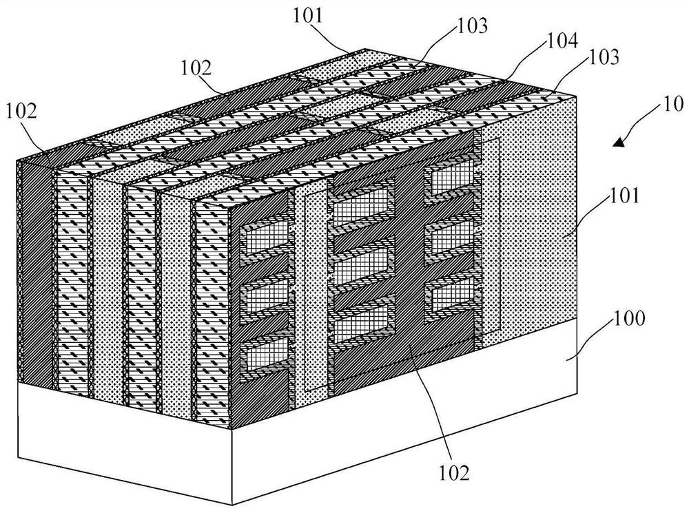
[0082] This embodiment provides a nanosheet field effect transistor, such as figure 1 As shown, the field effect transistor 10 includes a semiconductor substrate 100, and the semiconductor substrate 100 may be any semiconductor substrate commonly used in the field, such as a silicon substrate.

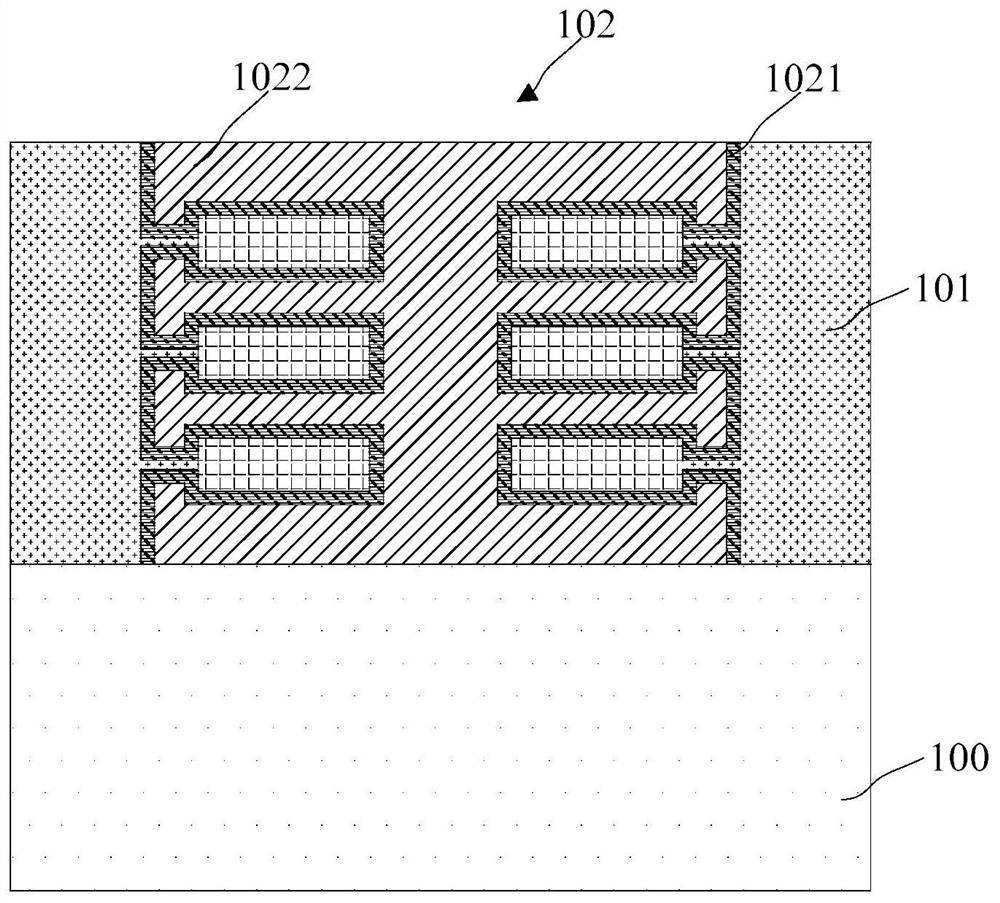
[0083] Insulation and isolation structures 110 are formed on the semiconductor substrate 100, and stacked multilayer nanosheets 105 are formed between the isolation and isolation structures 110, and the multilayer nanosheets 105 are spaced apart from each other. Such as figure 2 As shown, the stacked nanosheets 105 form a channel region. In this embodiment, an insulating isolation structure support portion 111 supporting the nanosheet 105 is formed between the nanosheet 105 and the insulating isolation structure 101 (see the attached Figure 10 ).

[0084] Such as figure 1 As shown, the nanosheet field effect transistor also has a gate structure 102 . The gate structure 102 is fo...

Embodiment 2

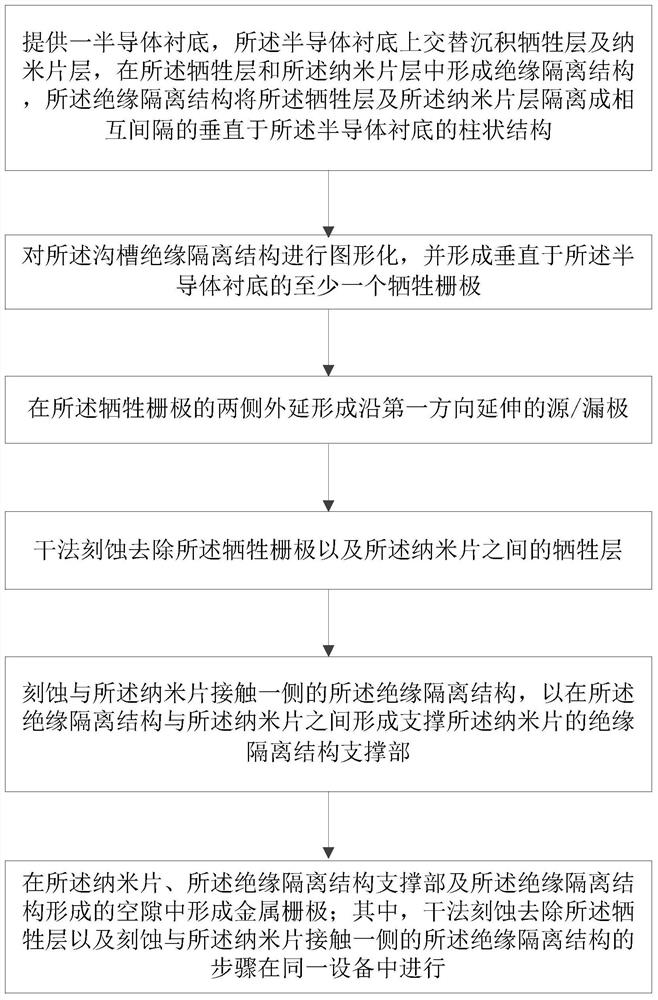
[0088] This embodiment provides a method for preparing a nanosheet field effect transistor, such as image 3 As shown, the method includes the following steps:

[0089] A semiconductor substrate is provided, on which a sacrificial layer and a nanosheet layer are alternately deposited, an insulating isolation structure is formed in the sacrificial layer and the nanosheet layer, and the insulating isolation structure separates the sacrificial layer and the nanosheet layer The nanosheets are isolated into columnar structures perpendicular to the semiconductor substrate spaced apart from each other;

[0090] patterning the insulating isolation structure, and forming at least one sacrificial gate perpendicular to the semiconductor substrate;

[0091] epitaxially forming source / drain extending along a first direction on both sides of the sacrificial gate;

[0092] dry etching to remove the sacrificial gate and the sacrificial layer between the nanosheets;

[0093] Etching the ins...


PUM

PropertyMeasurementUnit
heightaaaaaaaaaa

Abstract

The invention provides a nanosheet field effect transistor and a preparation method thereof, and the method comprises the steps: forming a nanosheet layer and a sacrificial layer on a semiconductor substrate, forming an insulation isolation structure in the nanosheet layer and the sacrificial layer, removing the sacrificial layer through dry etching, etching the insulation isolation structure, andforming a nanosheet supporting part; forming continuous gate insulating layers on the surfaces of the nanosheet and the nanosheet supporting part, and forming a second gate insulating layer between the gate insulating layers on the outer sides of the connecting parts, and forming a metal gate between the gate insulating layer and the second gate insulating layer. According to the invention, the sacrificial layer is removed and the insulation isolation structure is etched to form the nanosheet supporting structure in the same equipment, so the transportation or movement of the structure is avoided, and the nanosheet is prevented from being damaged due to factors such as physical vibration and the like. And the stability of the nanosheet is further improved by the gate insulating layer. Inaddition, dry etching is adopted in the method, and the damage, caused by chemical reagents, to the nanosheet is avoided.

Description

technical field [0001] The invention relates to the technical field of semiconductor integrated circuits, in particular to a nanosheet field effect transistor and a preparation method thereof. Background technique [0002] In integrated circuits, field effect transistors with low power and high operating performance usually have the following characteristics: (1) semiconductor substrate with high mobility; (2) increasingly larger channel width and smaller and smaller channel length; (3) a gate insulating layer with a large capacitance Ci; (4) reducing the interface traps at the interface between the active region channel and the gate insulating layer; (5) reducing the contact resistance between the electrode and the semiconductor layer. In recent years, the field effect transistor structure has undergone a remarkable change from planar type to 3D structures such as fin type or nanowire. [0003] New nanosheet field effect transistors, such as fork type nanosheet field effec...

Claims


Application Information

Patent Timeline
Patent Type & Authority Applications(China)
IPC IPC(8): H01L21/336H01L29/78H01L29/10B82Y10/00
CPCH01L29/6653H01L29/66545H01L29/7838H01L29/1033B82Y10/00
Inventor 三重野文健
Owner SIEN QINGDAO INTEGRATED CIRCUITS CO LTD
Why Eureka
Try Eureka