Unlock instant, AI-driven research and patent intelligence for your innovation.

Manufacturing method of three-dimensional memory

A manufacturing method and memory technology, applied in the direction of electric solid-state devices, semiconductor devices, electrical components, etc., can solve the problem of damage to the functional layer, failure of the storage function of the three-dimensional memory, easy misalignment between the second channel hole and the first channel hole, etc. problem, to achieve the effect of improving yield and reliability

Active Publication Date: 2020-10-09
YANGTZE MEMORY TECH CO LTD
View PDF4 Cites 0 Cited by
  • Summary
  • Abstract
  • Description
  • Claims
  • Application Information

AI Technical Summary

Problems solved by technology

[0004] However, in the process of manufacturing the above-mentioned three-dimensional memory, misalignment between the second channel hole and the first channel hole is prone to occur, resulting in that when the bottom of the functional layer is etched on the front side to form a through hole, it will damage the second channel hole. The functional layer at the junction of the channel hole and the first channel hole, which in turn causes the storage function of the three-dimensional memory to fail, reducing the yield and reliability of the three-dimensional memory

Method used


Image

  • Manufacturing method of three-dimensional memory
  • Manufacturing method of three-dimensional memory
  • Manufacturing method of three-dimensional memory

Examples


Embodiment 1

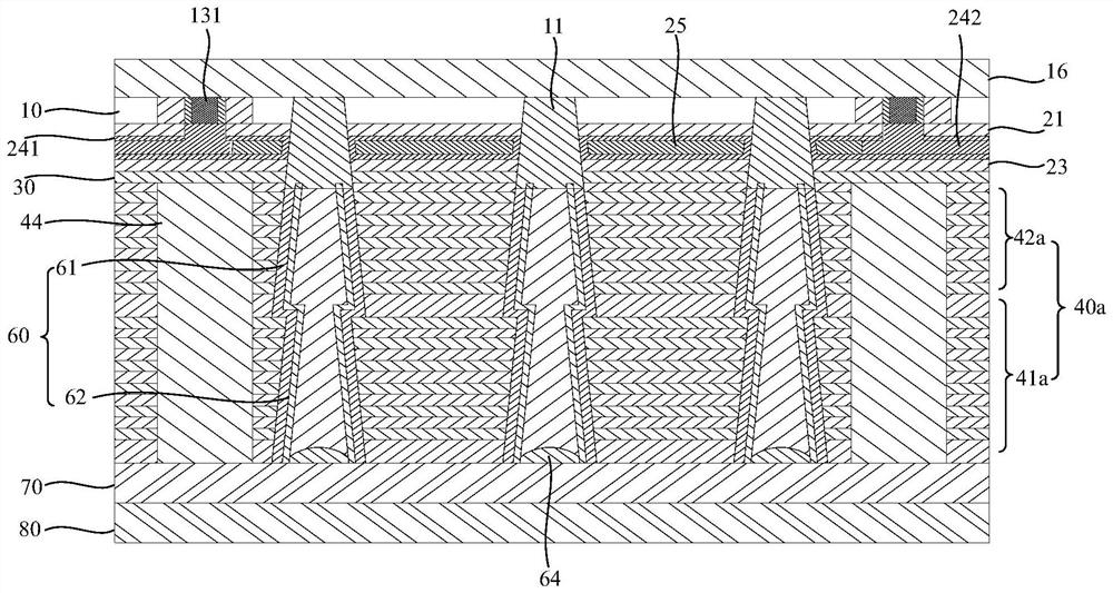
[0094] figure 1 It is a schematic structural diagram of a three-dimensional memory in an embodiment of the present invention; as figure 1 As shown, the three-dimensional memory provided by the embodiment of the present invention includes a substrate 10, and the substrate 10 can be made of a semiconductor material, and the manufacturing material of the substrate 10 includes but not limited to silicon, germanium, silicon germanium, etc. Made of single crystal silicon.

[0095] A stack structure 40a is disposed on the substrate 10; for example, a first stack structure 41a and a second stack structure 42a are sequentially disposed on the substrate 10, that is, the second stack structure 42a is located above the first stack structure 41a. Both the first stack structure 41a and the second stack structure 42a include a plurality of insulating layers and a plurality of gate layers alternately arranged; wherein, the thickness of the gate layer and the thickness of the insulating layer...

Embodiment 2

[0161] Figure 23 It is a schematic structural diagram of the three-dimensional memory in the second embodiment of the present invention; it should be noted that the structure of the three-dimensional memory provided in the second embodiment is the same as the structure of the three-dimensional memory provided in the first embodiment, and will not be repeated here. The difference between the structure of the three-dimensional memory provided in the second embodiment and the three-dimensional memory provided in the first embodiment is that, in the second embodiment, the etching barrier layer 30 and the substrate 10 are provided with the closest substrate The gate layer of the bottom 10 (that is, the first gate layer 25 located between the substrate 10 and the etch stop layer 30 in Embodiment 1), and the first channel structure 61 passes through the gate closest to the substrate 10 The gate layer extends into the substrate 10 , and a semiconductor layer 26 is provided on both si...

Embodiment 3

[0200] Figure 38 A schematic structural diagram of a three-dimensional memory provided in Embodiment 3 of the present invention; as Figure 38 As shown, the three-dimensional memory provided by this embodiment includes a substrate 10 and a first stack structure 41a and a second stack structure 42a disposed on the substrate 10 in sequence, wherein the first stack structure 41a is located on the substrate 10, and the second stack structure 42a is disposed on the substrate 10. The stack structure 42a is located on the first stack structure 41a, and the first stack structure 41a is provided with a first channel structure 61 perpendicular thereto, and one end of the first channel structure 61 close to the substrate 10 can extend to the end of the substrate 10 On the surface, the end of the first channel structure 61 away from the substrate 10 is electrically connected to the second channel structure 62 .

[0201] The structure of the first channel structure 61 and the second chan...


PUM

PropertyMeasurementUnit
thicknessaaaaaaaaaa
lengthaaaaaaaaaa

Abstract

The invention provides a manufacturing method of a three-dimensional memory, belongs to the technical field of semiconductor storage, and aims to solve the problem that a functional layer located at the joint of a first channel hole and a second channel hole is damaged when a channel structure located at the bottom of the channel hole is opened. According to the manufacturing method of the three-dimensional memory, a semiconductor layer is formed at the position closest to a gate layer of a substrate, the semiconductor layer penetrates through the gate layer closest to the substrate and is incontact with the substrate, and meanwhile, in the direction parallel to the substrate, the semiconductor layer penetrates through the functional layer and is electrically connected with a channel layer, so that the channel layer is in contact with the substrate through the semiconductor plunger and forms electric connection with the substrate. According to the manufacturing method of the three-dimensional memory provided by the invention, the functional layer at the joint of the second channel hole and the first channel hole can be prevented from being damaged while the electrical connection between the substrate and the channel layer is realized, and the yield and the reliability of the three-dimensional memory are improved.

Description

technical field [0001] The invention relates to the technical field of semiconductor storage, in particular to a method for manufacturing a three-dimensional memory. Background technique [0002] With the development of semiconductor memory devices, the demand for semiconductor memory devices with high-density data storage units is also continuously increasing; therefore, three-dimensional memory with multiple data storage unit layers stacked vertically has become a research hotspot. [0003] The three-dimensional memory includes a substrate and several stack structures stacked on the substrate. For example, two stack structures are stacked on the substrate: an upper stack structure and a lower stack structure; the upper stack structure is provided with a second channel The hole and the lower stack structure are provided with a first channel hole, and the second channel hole communicates with the first channel hole to form a channel hole that runs through the two stack struc...

Claims


Application Information

Patent Timeline
Patent Type & Authority Applications(China)
IPC IPC(8): H01L27/1157H01L27/11582H10B43/35H10B43/27
CPCH10B43/35H10B43/27
Inventor 徐伟杨星梅王健舻吴继君黄攀周文斌
Owner YANGTZE MEMORY TECH CO LTD