Power semiconductor device and manufacturing method thereof

A technology of power semiconductors and semiconductors, applied in semiconductor/solid-state device manufacturing, semiconductor devices, electrical components, etc.

Inactive Publication Date: 2020-10-09
HANGZHOU SILAN MICROELECTRONICS +1
View PDF0 Cites 0 Cited by
  • Summary
  • Abstract
  • Description
  • Claims
  • Application Information

AI Technical Summary

Problems solved by technology

When the power device is turned on and off, this part of the extra capacitor needs to be charged and discharged, resulting in additional loss

Method used


Image

  • Power semiconductor device and manufacturing method thereof
  • Power semiconductor device and manufacturing method thereof
  • Power semiconductor device and manufacturing method thereof

Examples


Embodiment Construction

[0074] Various embodiments of the invention will be described in more detail below with reference to the accompanying drawings. In the various drawings, the same elements are denoted by the same or similar reference numerals. For the sake of clarity, various parts in the drawings have not been drawn to scale.

[0075]Below in conjunction with accompanying drawing and embodiment, the specific embodiment of the present invention is described in further detail.

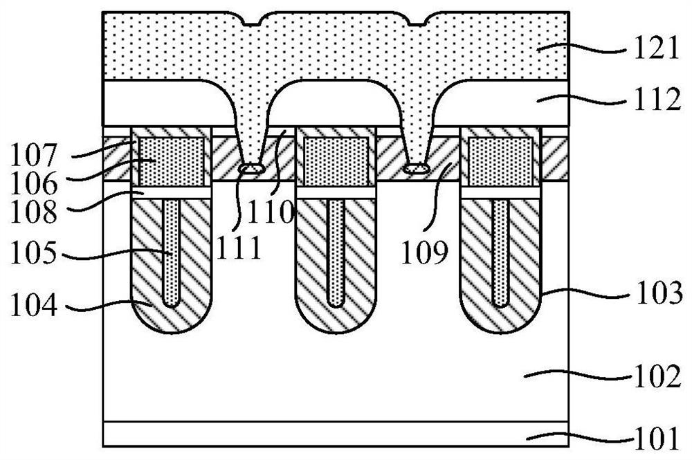
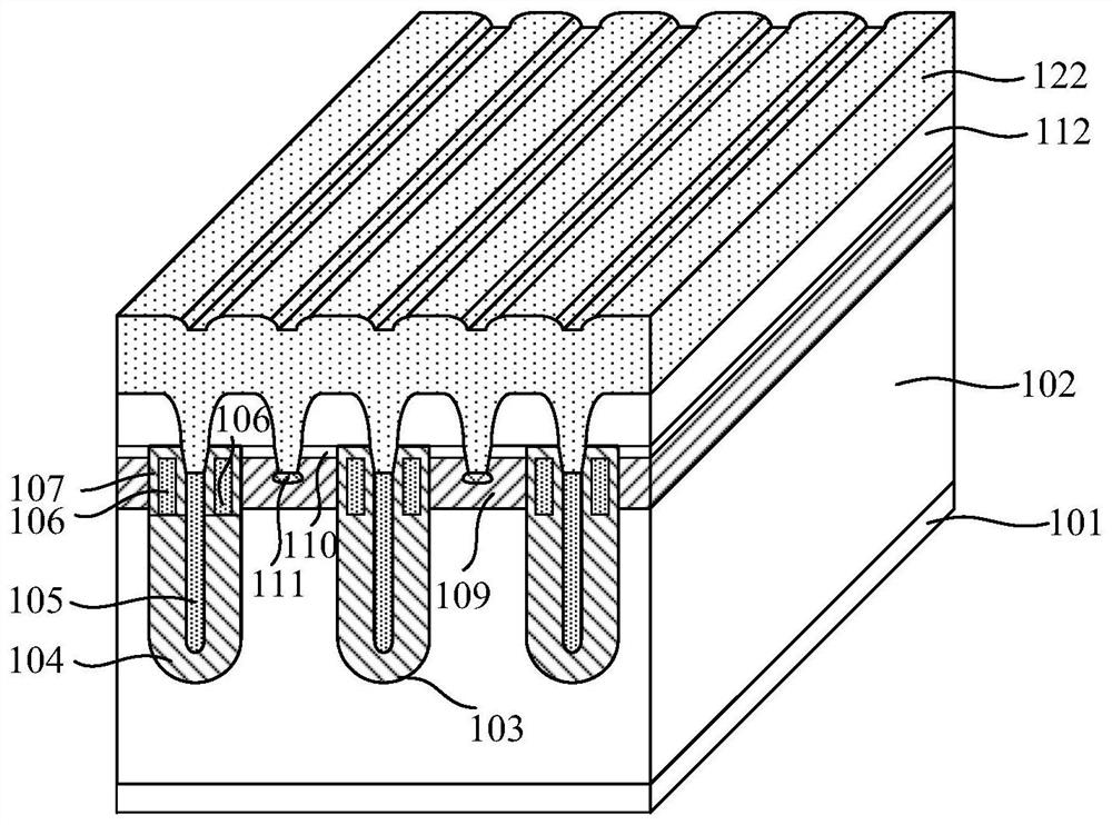
[0076] In the power semiconductor device described in the following embodiments, the shielding conductor in one groove has multiple lead-out positions in the longitudinal direction of the groove, so as to solve the problem of the two ends of the shielding conductor lead-out position in the longitudinal direction of the groove in the traditional structure. The excessively long terminal distance leads to the problem of excessively large parasitic resistance of the shielding conductor.

[0077] Figure 4 A schematic diag...


PUM

PropertyMeasurementUnit
thicknessaaaaaaaaaa
thicknessaaaaaaaaaa
thicknessaaaaaaaaaa

Abstract

The invention discloses a power semiconductor device and a manufacturing method thereof. A part of a shielding conductor of the power semiconductor device is connected with a source electrode, the shielding conductor extends from the bottom of a groove to the position between gate conductors on the two sides in the groove at the position electrically connected with the source electrode, the gate conductors and the shielding conductor are separated by an isolation layer, and the shielding conductor is connected with the source electrode; part of the shielding conductor is not connected with thesource electrode, and the shielding conductor extends from the bottom of the trench to the area below the gate conductors on the two sides of the upper portion of the trench at the position where theshielding conductor is not electrically connected with the source electrode, so that parasitic resistance of the shielding conductor is reduced, and parasitic resistance is reduced by dozens of times.

Description

technical field [0001] The invention relates to the technical field of semiconductor manufacturing, in particular to a power semiconductor device and a manufacturing method thereof. Background technique [0002] Power semiconductor devices are also known as power electronic devices, including power diodes, thyristors, VDMOS (Vertical double-diffused metal oxide semiconductor, vertical double-diffused metal oxide semiconductor) field effect transistors, LDMOS (Laterally diffused metal oxide semiconductor, laterally diffused metal oxide semiconductor) material semiconductor) field effect transistor and IGBT (Insulated gate bipolar transistor, insulated gate bipolar transistor), etc. A VDMOS field effect transistor includes a source region and a drain region formed on opposite surfaces of a semiconductor substrate, and in an on state, current flows mainly along the longitudinal direction of the semiconductor substrate. [0003] In the high-frequency application of power semico...

Claims


Application Information

Patent Timeline
Patent Type & Authority Applications(China)
IPC IPC(8): H01L29/06H01L29/423H01L29/78H01L21/336
CPCH01L29/0603H01L29/0684H01L29/42356H01L29/66712H01L29/7802
Inventor 张邵华郭广兴杨彦涛
Owner HANGZHOU SILAN MICROELECTRONICS
Why Eureka
Try Eureka