
Broadband periodic wave-absorbing structure based on magnetic substrate

A magnetic substrate and wave structure technology, applied in electrical components, antennas and other directions, can solve the problem that the low-frequency broadband absorbing effect cannot meet the application requirements, etc., to improve the low-frequency broadband absorbing effect, low production cost, structure and preparation process. simple effect

Active Publication Date: 2020-10-09
UNIV OF ELECTRONICS SCI & TECH OF CHINA
View PDF5 Cites 3 Cited by
  • Summary
  • Abstract
  • Description
  • Claims
  • Application Information

AI Technical Summary

Problems solved by technology

[0005] The present invention aims at the deficiencies in the above-mentioned prior art, in order to solve the problem that the low-frequency broadband absorbing effect of the existing absorbing materials cannot meet the application requirements after reducing the structural thickness, and provides a broadband periodic absorbing based on a magnetic substrate The structure realizes the thinning of the broadband absorbing material, and also improves the low-frequency broadband absorbing effect

Method used


Image

  • Broadband periodic wave-absorbing structure based on magnetic substrate
  • Broadband periodic wave-absorbing structure based on magnetic substrate
  • Broadband periodic wave-absorbing structure based on magnetic substrate

Examples


Embodiment 1

[0027] Such as Figure 4 As shown, when the TE wave or TM wave is vertically incident, the broadband periodic absorbing structure based on the magnetic substrate made by the above content is used for simulation. The simulation result is: in the whole frequency band of 0.5-18GHz, it has a reflection coefficient of at least -6dB or less , where the 1-5GHz frequency band has a reflection coefficient below -10dB.

Embodiment 2

[0029] Such as Figure 5 As shown, when the TE wave and TM wave are incident at 30°, the broadband periodic absorbing structure based on the magnetic base rubber sheet made by the above content is used for simulation. The simulation result is: both modes have Reflection coefficient below at least -4dB, among which TM mode in the 1-10GHz frequency band has a reflection coefficient below -6dB, and TE mode in the 1-8GHz frequency band has a reflection coefficient below -10dB.

Embodiment 3

[0031] Such as Figure 6 As shown, when the TE wave and TM wave are incident at 45°, the broadband periodic absorbing structure based on the magnetic base rubber sheet made by the above content is used for simulation. The simulation results are: in the 1-18GHz frequency band, the TE wave has at least -8dB The reflection coefficient below TM wave has a reflection coefficient below -4dB in the 1-18GHz frequency band.


PUM

PropertyMeasurementUnit
thicknessaaaaaaaaaa
thicknessaaaaaaaaaa
thicknessaaaaaaaaaa

Abstract

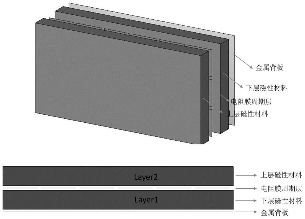
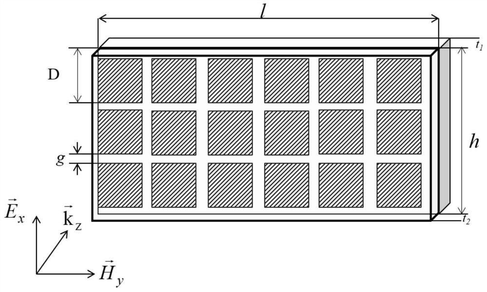
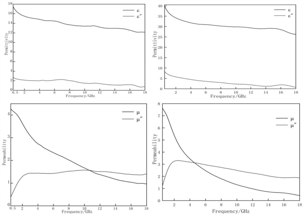
The invention discloses a broadband periodic wave-absorbing structure based on a magnetic substrate, and belongs to the technical field of electronic materials. The broadband periodic wave-absorbing structure comprises an upper magnetic material layer, a lower magnetic material layer and a resistive film periodic layer arranged on a support of the two magnetic material layers to form a wave-absorbing body, wherein the upper magnetic material layer and the lower magnetic material layer are both flexible magnetic wave-absorbing rubber plates, and the dielectric constant and the magnetic conductivity of the upper magnetic material layer are both lower than those of the lower magnetic material layer. According to the broadband periodic wave-absorbing structure based on the magnetic substrate,the low-frequency broadband wave-absorbing effect is improved while the broadband wave-absorbing material is thinned. And the structure and the preparation process are simple, so that the manufacturing cost is low, and the operability is high.

Description

technical field [0001] The invention belongs to the technical field of electronic materials, and in particular relates to a broadband periodic wave-absorbing structure based on a magnetic substrate. Background technique [0002] During World War II, the widespread use of radar as an advanced long-range detection tool gave birth to the emergence of radar stealth technology. In modern warfare, the electromagnetic environment is becoming more and more complex, and radar absorbing materials, as an effective means to improve the stealth penetration capability of weapons and equipment, have also received more and more attention from various military powers. In addition, with the widespread use of technical products such as mobile phones and microwave ovens that use electromagnetic waves as a medium in various fields of real life, the accompanying electromagnetic pollution such as electromagnetic radiation also poses a threat to human survival and health. Therefore, radar absorbin...

Claims


Application Information

Patent Timeline
Patent Type & Authority Applications(China)
IPC IPC(8): H01Q17/00
CPCH01Q17/00H01Q17/007H01Q17/008
Inventor 梁迪飞蒋文颖刘倩李维佳
Owner UNIV OF ELECTRONICS SCI & TECH OF CHINA
Learn More