
A cmos pixel sensor

A pixel sensor and pixel technology, applied in image communication, electric solid-state devices, semiconductor devices, etc., can solve the problems of low collection efficiency and long charge collection time, and achieve the goal of increasing the collection area, improving the charge collection efficiency, and increasing the amplifier gain Effect

Active Publication Date: 2021-10-08
SHANDONG UNIV
View PDF6 Cites 0 Cited by
  • Summary
  • Abstract
  • Description
  • Claims
  • Application Information

AI Technical Summary

Problems solved by technology

[0003] However, the inventors found that the pixels in the CMOS pixel sensor use small-area diodes to collect charges, and the ratio of the diode area to the pixel unit is relatively small, resulting in the charge being recombined during the collection process, resulting in longer charge collection time and lower collection efficiency.

Method used


Image

  • A cmos pixel sensor
  • A cmos pixel sensor
  • A cmos pixel sensor

Examples


Embodiment Construction

[0030] It should be noted that the following detailed description is exemplary and intended to provide further explanation of the present invention. Unless defined otherwise, all technical and scientific terms used herein have the same meaning as commonly understood by one of ordinary skill in the art to which this invention belongs.

[0031] It should be noted that the terminology used here is only for describing specific embodiments, and is not intended to limit exemplary embodiments according to the present invention. As used herein, unless the invention clearly states otherwise, the singular form is also intended to include the plural form. In addition, it should also be understood that when the terms "comprising" and / or "comprising" are used in this specification, their Indicate the presence of features, steps, operations, means, components and / or combinations thereof;

[0032] Explanation of terms:

[0033] CMOS: Complementary Metal Oxide Semiconductor, Complementary M...


PUM

PropertyMeasurementUnit
electrical resistivityaaaaaaaaaa

Abstract

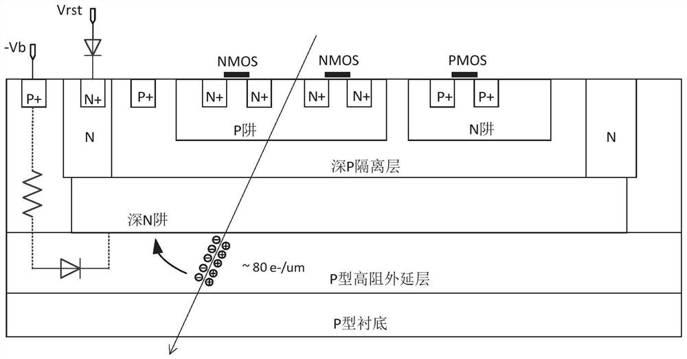
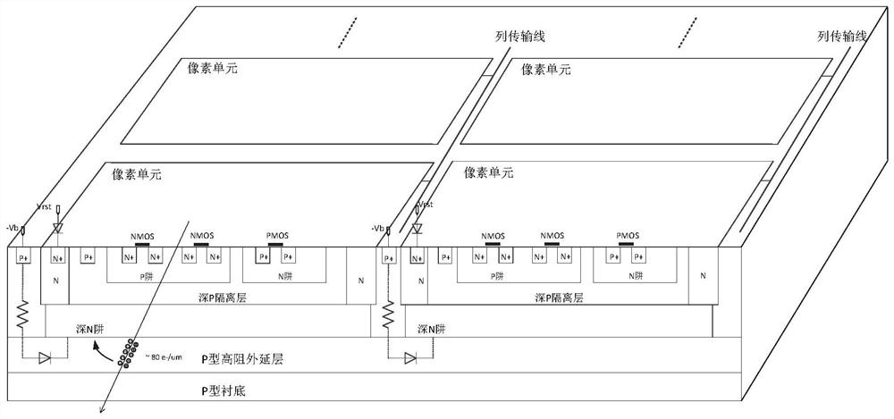
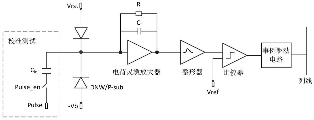
The invention discloses a CMOS pixel sensor, which comprises a P-type substrate, a P-type high resistance epitaxial layer, an N well, a P well, a deep N well and a deep P isolation layer; wherein, the deep N well and the P-type high resistance epitaxial layer Form a P-N diode; the N well on the deep N well and the N-type active region form a channel, and connect other readout circuits through metal lines; the deep P isolation layer is used to isolate the devices in the deep N well, and the deep P isolation layer The N-well and P-type active region in the deep P-isolation layer are used to make PMOS transistors, and the P-well and N-type active region in the deep P isolation layer are used to make NMOS transistors.

Description

technical field [0001] The invention relates to the field of semiconductor integrated circuits, and relates to a CMOS pixel sensor. Background technique [0002] With the development of semiconductor technology industry and lithography technology, CMOS pixel sensors are more and more widely used in X-ray imaging and particle detection, which have high spatial resolution, fast readout speed, high integration, low power consumption and Low cost and other characteristics have gradually become an important detection technology. [0003] However, the inventors found that the pixels in the CMOS pixel sensor use small-area diodes to collect charges, and the ratio of the diode area to the pixel unit is small, resulting in the charge being recombined during the collection process, resulting in longer charge collection time and lower collection efficiency. Contents of the invention [0004] In view of the deficiencies in the prior art, the object of the present invention is to prov...

Claims


Application Information

Patent Timeline
Patent Type & Authority Patents(China)
IPC IPC(8): H01L27/146H04N5/374
CPCH01L27/14605H01L27/14612H01L27/1461H01L27/14643H04N25/76
Inventor 张亮王萌董家宁王安庆李龙
Owner SHANDONG UNIV
Learn More