A kind of igbt device and manufacturing method thereof
A device and semiconductor technology, which is applied in the field of insulated gate bipolar transistor devices and its manufacturing, can solve the problems of limiting IGBT performance, IGBT avalanche current and voltage characteristics, and IGBT’s limited withstand voltage capability, so as to improve reliability and reverse Effects of breakdown voltage and stability improvement
- Summary
- Abstract
- Description
- Claims
- Application Information
AI Technical Summary
Problems solved by technology
Method used
Image
Examples
Embodiment 1
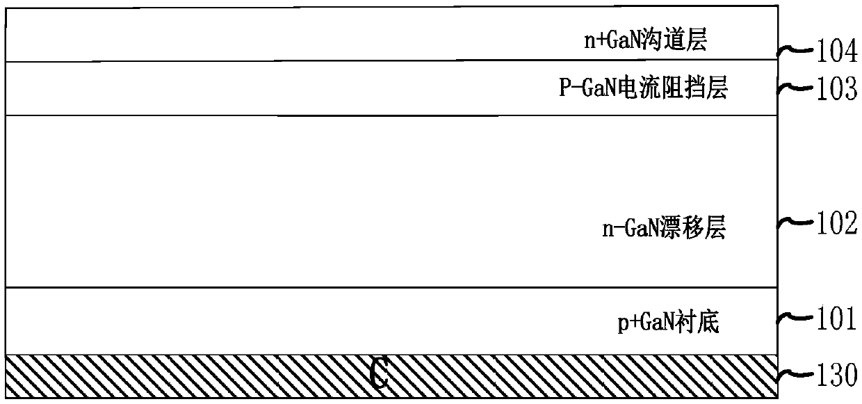
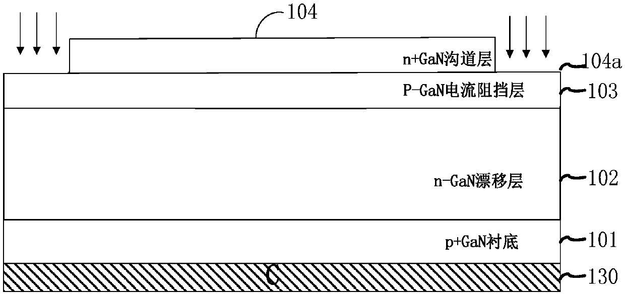
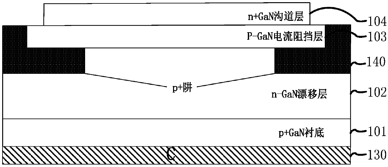
[0048] Embodiment 1, with reference to Figure 1A-Figure 1G shown
[0049] The manufacturing method of the IGBT provided in this embodiment, such as Figure 1A As shown, firstly, step S1 is performed to sequentially grow a drift layer 102 , a current blocking layer 103 , and a semiconductor channel layer 104 on a substrate 101 . Wherein, the bottom layer is the substrate 101, and the substrate 101 can be formed by heavily doped B or implantation process. In this embodiment, the substrate 101 is a heavily doped p+GaN semiconductor layer. In other embodiments, the substrate 101 can also be other heavily doped semiconductor materials; further, the drift layer 102 can be a lightly doped n-GaN layer; the current blocking layer 103 can be a p-GaN layer; the semiconductor channel layer 104 can be a heavily doped n+GaN layer. A drift layer 102 is grown on the substrate 101. In this embodiment, the drift layer 102 is a lightly doped n-GaN semiconductor layer. The current blocking la...
Embodiment 2
[0063] Embodiment 2, with reference to figure 2 shown
[0064] figure 2 It is a schematic diagram of a modified structure of Embodiment 1 of the present invention. like figure 2 As shown, on the basis of Embodiment 1, a two-dimensional electron gas re-growth layer 180 is formed in the semiconductor channel layer 104 between the emitter electrodes 105 and the gate trench 120 by material growth equipment. The two-dimensional electron gas regrowth layer 180 includes an electron transport semiconductor layer 106 and an electron supply semiconductor layer 107 located on the electron transport semiconductor layer 106, forming a two-dimensional Electron Gas108. The two-dimensional electron gas 108 is formed in the electron transport semiconductor layer 106 at the interface between the electron supply semiconductor layer 107 and the electron transport semiconductor layer 106 due to the polarization effect. In other embodiments of the present invention, the electron supply semi...
Embodiment 3
[0068] Embodiment 3, with reference to image 3 shown
[0069] The IGBT device 100 obtained through the above design can basically meet the requirements of use, but for the purpose of further improving its functions, the designer has made further improvements to the IGBT device 100 .
[0070] In this embodiment, on the basis of the device structure in Embodiment 2, a buffer layer 160 is formed before growing the drift layer 102 on the substrate 101, and then the drift layer 102 is formed on the buffer layer 160. The subsequent steps are the same as in Embodiment 2. same. That is to say, in the IGBT device structure of the second embodiment, the buffer layer 160 is inserted between the drift layer 102 and the substrate 101 to form a punch-through (PT) IGBT structure 200 . In other preferred embodiments of the present invention, the buffer layer is a heavily doped n+GaN layer. Since the heavily doped n+GaN layer is heavily doped or injected with electrons, the forward conduct...
PUM
 Abstract
Description
Claims
Application Information


