sno 2 Self-driven ultraviolet photodetector based on homojunction and its preparation method
A photodetector and homojunction technology, applied in circuits, electrical components, semiconductor devices, etc., can solve the problems of slow response speed and high dark current, and achieve the effects of low dark current, fast response speed, and good rectification characteristics
- Summary
- Abstract
- Description
- Claims
- Application Information
AI Technical Summary
Problems solved by technology
Method used
Image
Examples
Embodiment 1
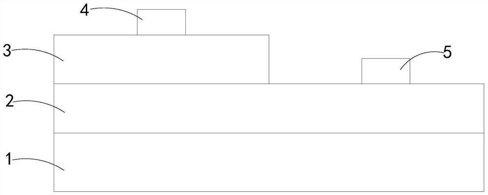
[0050] like figure 1 As shown, the present invention provides a SnO 2 Homojunction-based self-driven UV photodetectors, including:
[0051] substrate1;
[0052] n-NbSnO 2 Thin film layer 2, located on the surface of substrate 1;
[0053] Mg-doped p-type conductive MgSnO 2 Thin film layer 3, on n-NbSnO 2 The surface of the thin film layer 2 away from the substrate, Mg-doped p-type conductive MgSnO 2 Thin film layer 3 on n-NbSnO 2 The orthographic projection of the surface of thin film layer 2 does not completely cover n-NbSnO 2 film layer 2;
[0054] The first metal electrode layer 4 is located on Mg-doped p-type conductive MgSnO 2 The surface of the film layer 3 away from the substrate 1 side;
[0055] The second metal electrode layer 5 is located on n-NbSnO 2 The thin film layer 2 is away from the substrate 1 and is not Mg-doped with p-type conductive MgSnO 2 Surface covered with film layer 3 .
[0056] It should be noted that, in the embodiment of the present ap...
Embodiment 2
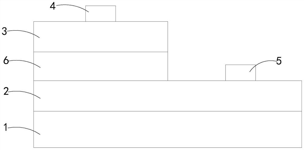
[0072] like image 3 As shown, the present invention provides a SnO 2 Self-driven UV photodetectors based on homogeneous pn junctions, including:
[0073] substrate1;
[0074] n-NbSnO 2 Thin film layer 2, located on the surface of substrate 1;
[0075] n-SnO 2 Thin film layer 6, located on NbSnO 2 The surface of the thin film layer 2 away from the substrate 1 side, n-SnO 2 Thin film layer 6 on n-NbSnO 2 The orthographic projection of the surface of thin film layer 6 does not completely cover n-NbSnO 2 film layer 6;
[0076] Mg-doped p-type conductive MgSnO 2 Thin film layer 3, on the n-SnO 2 The surface of the film layer 6 away from the substrate 1 side;
[0077] The first metal electrode layer 4 is located on Mg-doped p-type conductive MgSnO 2 The surface of the film layer 3 away from the substrate 1 side;
[0078] The second metal electrode layer 5 is located on n-NbSnO 2 The thin film layer 2 is away from the substrate 1 side and is not covered by n-SnO 2 The...
PUM
 Abstract
Description
Claims
Application Information


