Multi-junction germanium-based long-wave infrared detector and preparation method thereof
A long-wave infrared and detector technology, used in electrical radiation detectors, radiation pyrometry, instruments, etc., can solve problems such as the difficulty of widening, and achieve low preparation cost, large depletion zone width, and good detection performance. Effect
- Summary
- Abstract
- Description
- Claims
- Application Information
AI Technical Summary
Problems solved by technology
Method used
Image

Examples
example 1
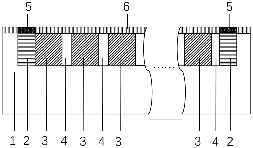
[0029] Select the high-resistance Ge substrate 1, and the doping concentration is 1×10 13 cm -3 , making two absorption region patterns on the surface of the Ge substrate 1 by means of ultraviolet lithography technology, the width of a single absorption region is 50 μm, and the thickness of the photoresist used is about 3 μm, which can be used as a masking agent for the subsequent ion implantation process;
[0030] Through multiple ion implantation processes, implant B impurities into the absorption region 3, the implantation depth is about 1 μm, and the doping concentration is about 4×10 16 cm -3 ;
[0031] Fabricate an electrode area pattern on the surface of the Ge substrate 1 by means of ultraviolet lithography again, and the width of the electrode area is 100 μm;
[0032] Through multiple ion implantation processes again, implant B impurities into the electrode region 2, the implantation depth is about 1 μm, and the doping concentration is about 3×10 18 cm -3 ;
[0...
example 2
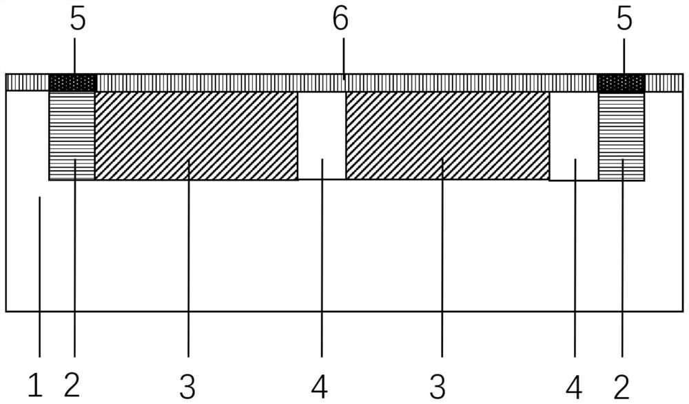
[0037] Select the high-resistance Ge substrate 1, and the doping concentration is 1×10 13 cm -3 , making five absorption region patterns on the surface of Ge substrate 1 by means of ultraviolet lithography technology, the width of a single absorption region is 20 μm, and the thickness of the photoresist used is about 3 μm, which can be used as a masking agent for the subsequent ion implantation process;
[0038] Through multiple ion implantation processes, implant B impurities into the absorption region 3, the implantation depth is about 1 μm, and the doping concentration is about 5×10 16 cm -3 ;
[0039] Fabricate an electrode area pattern on the surface of the Ge substrate 1 by means of ultraviolet lithography again, and the width of the electrode area is 100 μm;
[0040] Through multiple ion implantation processes again, implant B impurities into the electrode region 2, the implantation depth is about 1 μm, and the doping concentration is about 3×10 18 cm -3 ;
[0041...
example 3
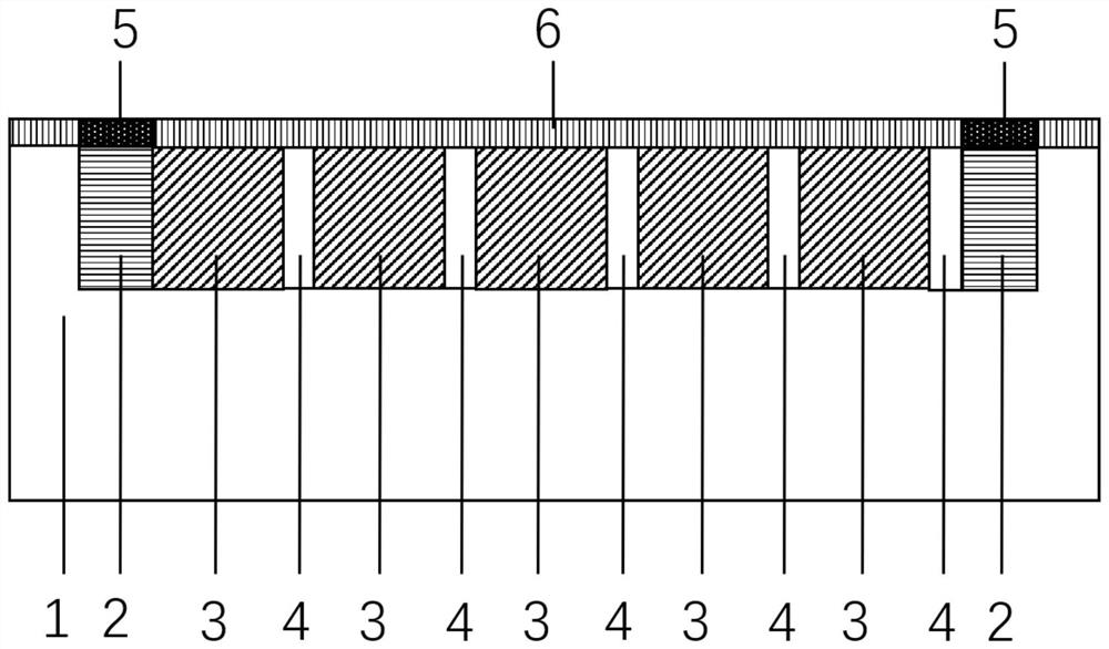
[0045] Select the high-resistance Ge substrate 1, and the doping concentration is 1×10 13 cm -3 , making ten absorption region patterns on the surface of the Ge substrate 1 by means of ultraviolet lithography technology, the width of each absorption region is 10 μm, and the thickness of the photoresist used is about 3 μm, which can be used as a masking agent for the subsequent ion implantation process;
[0046] Through multiple ion implantation processes, implant B impurities into the absorption region 3, the implantation depth is about 1 μm, and the doping concentration is about 2×10 16 cm -3 ;
[0047] Fabricate an electrode region pattern on the surface of the Ge substrate 1 again by means of ultraviolet lithography technology, and the width of the electrode region is 100 μm;
[0048] Through multiple ion implantation processes again, implant B impurities into the electrode region 2, the implantation depth is about 1 μm, and the doping concentration is about 3×10 18 cm ...
PUM
| Property | Measurement | Unit |
|---|---|---|
| Width | aaaaa | aaaaa |
Abstract
Description
Claims
Application Information