Coil structure and semiconductor processing equipment

A processing equipment and semiconductor technology, applied in coils, semiconductor/solid-state device manufacturing, discharge tubes, etc., can solve problems such as uneven plasma, etching quality or adverse effects on efficiency, and achieve the effect of improving etching quality

Inactive Publication Date: 2020-10-16
BEIJING NAURA MICROELECTRONICS EQUIP CO LTD
View PDF0 Cites 3 Cited by
  • Summary
  • Abstract
  • Description
  • Claims
  • Application Information

AI Technical Summary

Problems solved by technology

[0004] The problem solved by the present invention is that in the prior art, the unevenness of the plasma produced by the coil has a bad influence on the etching quality or efficiency

Method used


Image

  • Coil structure and semiconductor processing equipment
  • Coil structure and semiconductor processing equipment
  • Coil structure and semiconductor processing equipment

Examples


Embodiment Construction

[0069] In order to make the above objects, features and advantages of the present invention more comprehensible, specific embodiments of the present invention will be described in detail below in conjunction with the accompanying drawings. It should be understood that the specific embodiments described here are only used to explain the present invention, not to limit the present invention.

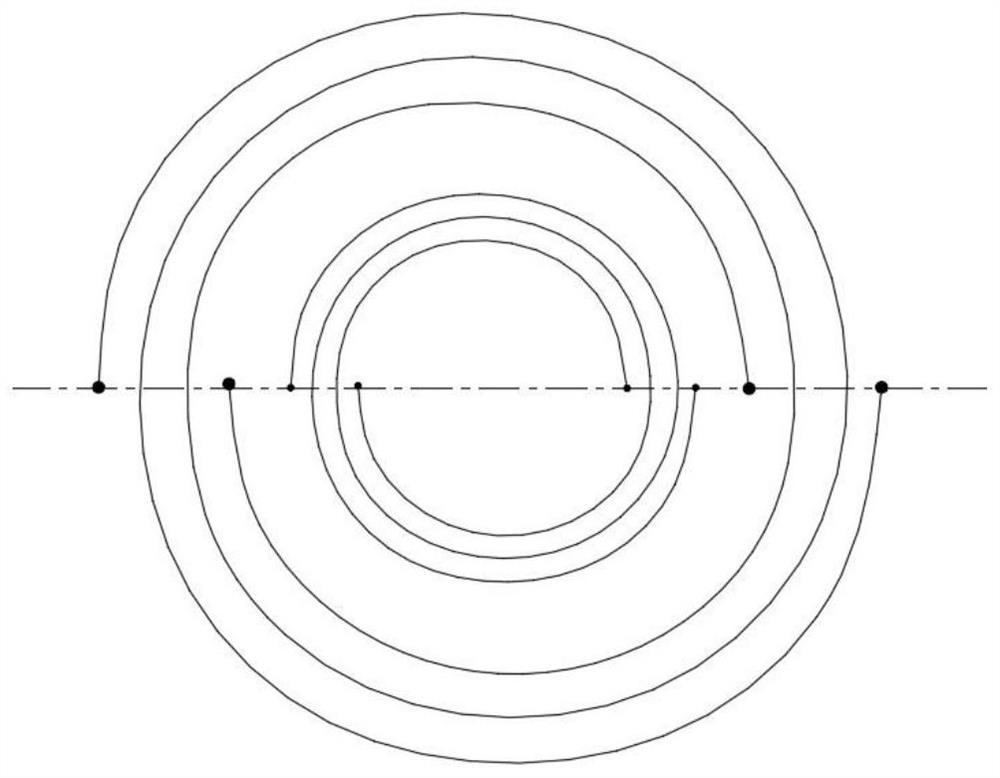
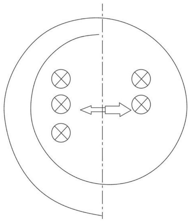
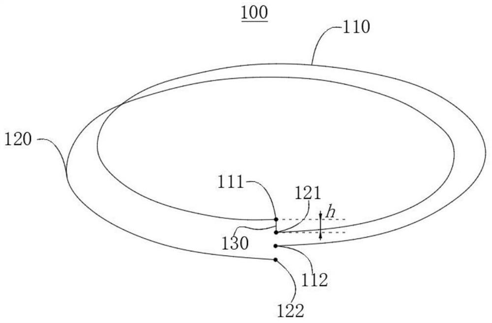
[0070] An embodiment of the present invention provides a coil structure for semiconductor devices, such as Figure 3-Figure 23 shown.

[0071] Such as Figure 3-Figure 5 , Figure 8 , Figure 11 , Figure 14-Figure 16 , Figure 22 As shown, the coil structure includes at least one coil group 100 .

[0072] Please continue to see Figure 3-Figure 5 , Figure 8 , Figure 11 , Figure 14-Figure 16 , Figure 22 , the coil set 100 includes a first coil 110 and a second coil 120, and the first coil 110 and the second coil 120 are wound to form a ring-shaped area (such as Figure 5 , ...


PUM


Abstract

The invention relates to the technical field of semiconductors, in particular to a coil structure. The coil structure comprises at least one coil assembly. The coil assembly comprises a first coil anda second coil, wherein the first coil and the second coil are wound to form an annular area, the first end of the first coil and the first end of the second coil are both gradually close to an innerring of the annular area, and the second end of the first coil and the second end of the second coil are both gradually close to an outer ring of the annular area; the first end of the first coil is electrically connected with the first end of the second coil, or the second end of the first coil is electrically connected with the second end of the second coil; the first coil forms a first projection on a plane perpendicular to the axial direction of the coil structure, the second coil forms a second projection on a plane perpendicular to the axial direction of the coil structure, and the firstprojection and the second projection are in mirror symmetry. The coil structure can produce uniform plasmas, and the etching quality and the etching efficiency of a semiconductor are effectively improved.

Description

technical field [0001] The invention relates to the technical field of semiconductors, in particular to a coil structure and semiconductor processing equipment. Background technique [0002] With the development of integrated circuit manufacturing technology, the requirements for the uniformity of the etching environment are getting higher and higher. In the etching process, the upper electrode is usually used to excite and generate plasma, and its distribution determines the uniformity of etching. Therefore, the coil structure used to generate plasma is very important for the uniformity of the etching process. [0003] In the prior art, usually such as figure 1 , figure 2 coil shown. in, figure 1 Among them, the coil is divided into inner and outer coil groups and both the inner and outer coil groups are planar structures, and the inner and outer coil groups are formed by parallel connection of two coils. figure 2 , a single coil is wound into asymptotes or concentri...

Claims


Application Information

Patent Timeline
Patent Type & Authority Applications(China)
IPC IPC(8): H01J37/32H01L21/67H01F5/00H01F5/04
CPCH01J37/3211H01L21/67069H01F5/00H01F5/04H01J37/321H01J2237/334H01J2237/3343
Inventor 韦刚陈星牛晨
Owner BEIJING NAURA MICROELECTRONICS EQUIP CO LTD
Why Eureka
Try Eureka