

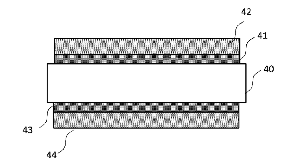
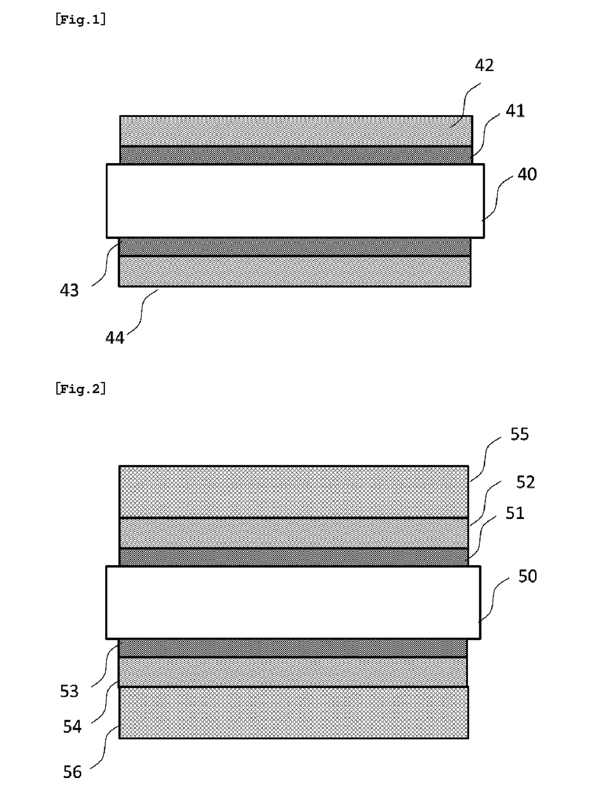
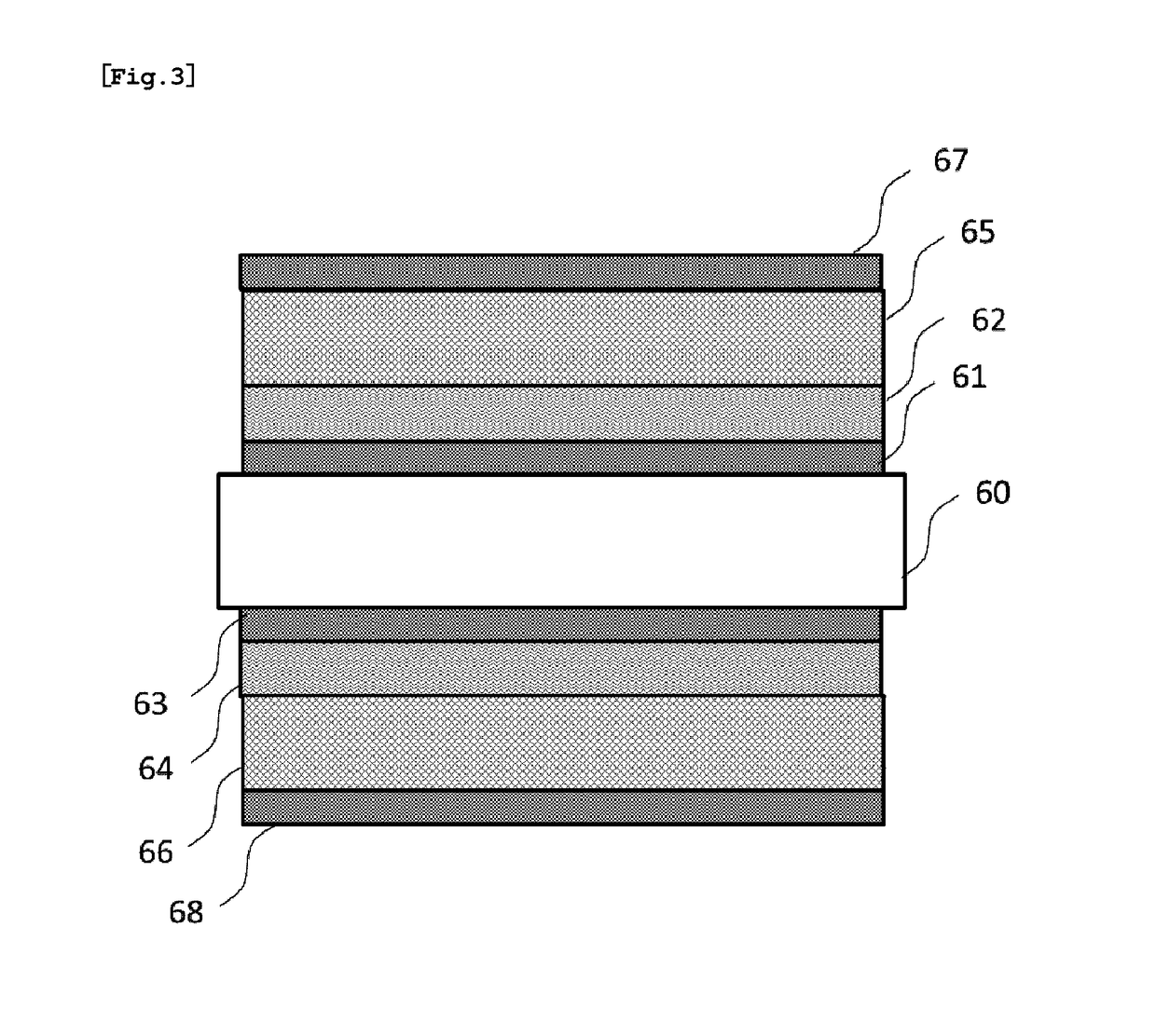
Laminate film and electrode substrate film, and method of manufacturing the same
a technology of laminate film and electrode substrate, which is applied in the direction of dielectric characteristics, instruments, and semiconductor/solid-state device details, etc., can solve the problems of deterioration, decreased product value, and opaque conductive film, and achieve excellent etching quality and avoid the effect of deterioration
- Summary
- Abstract
- Description
- Claims
- Application Information
AI Technical Summary
Benefits of technology
Problems solved by technology
Method used
Image

Examples
examples
[0168]Hereinbelow, examples of the present invention are described in detail with reference to a comparative example. Note that the present invention is not limited to the examples to be described later.
examples 1 to 5
[0169]The deposition apparatus (sputtering web coater) illustrated in FIG. 5 is used and oxygen gas is used as the reactive gas. In addition, the can roll 16 is made of stainless steel with a diameter of 600 mm and a width of 750 mm, and a surface of the roll is plated with hard chrome. Each of the upstream feed roll 15 and the downstream feed roll 21 is made of stainless steel with a diameter of 150 mm and a width of 750 mm, and a surface of each roll is plated with hard chrome. Besides, the gas discharge pipes 25, 26, 27, 28, 29, 30, 31, and 32 were installed on the upstream side and the downstream side of the magnetron sputtering cathodes 17, 18, 19, and 20. Moreover, a Ni—Cu target for the metal absorption layer was attached to the magnetron sputtering cathodes 17 and 18, and a Cu target for the metal layer to the magnetron sputtering cathodes 19 and 20.
[0170]Note that the magnetron sputtering cathodes 17 and 18 of FIG. 5 correspond to the magnetron sputtering cathodes 117 and 1...
PUM
| Property | Measurement | Unit |
|---|---|---|
| thickness | aaaaa | aaaaa |
| width | aaaaa | aaaaa |
| thickness | aaaaa | aaaaa |
Abstract
Description
Claims
Application Information