Manufacturing method of semiconductor device

A manufacturing method and semiconductor technology, applied in semiconductor/solid-state device manufacturing, semiconductor devices, electrical components, etc., can solve problems such as saturation gate current failure

Pending Publication Date: 2020-10-16
SHANGHAI HUAHONG GRACE SEMICON MFG CORP
View PDF0 Cites 6 Cited by
  • Summary
  • Abstract
  • Description
  • Claims
  • Application Information

AI Technical Summary

Problems solved by technology

[0017] The purpose of the present invention is to provide a method for manufacturing a semiconductor device to solve the pr

Method used


Image

  • Manufacturing method of semiconductor device
  • Manufacturing method of semiconductor device
  • Manufacturing method of semiconductor device

Examples


Embodiment Construction

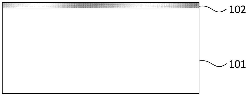
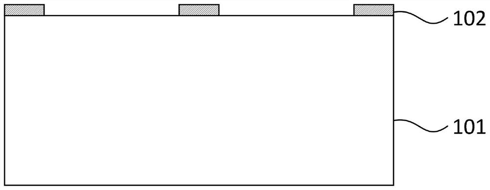
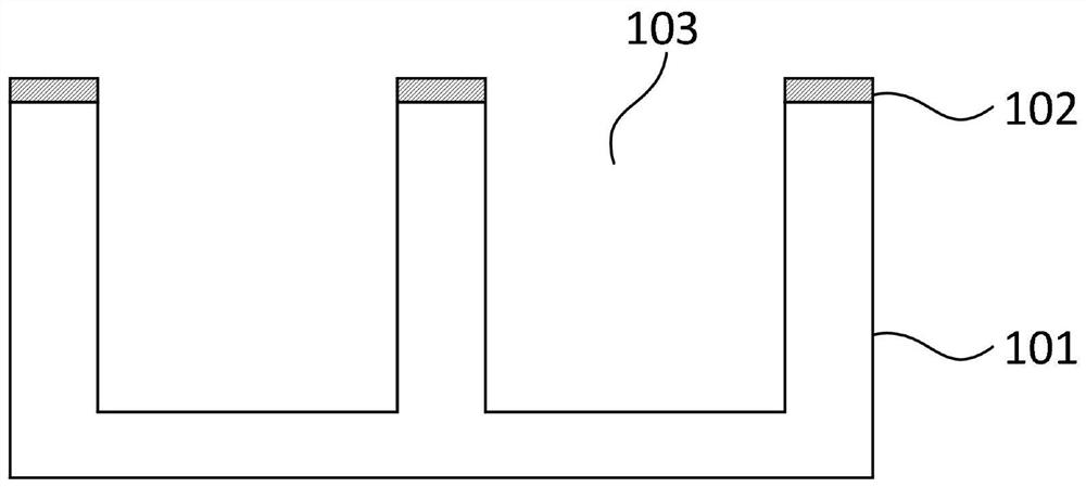
[0056] The manufacturing method of the semiconductor device proposed by the present invention will be further described in detail below with reference to the accompanying drawings and specific embodiments. It should be noted that all the drawings are in a very simplified form and use imprecise scales, and are only used to facilitate and clearly assist the purpose of illustrating the embodiments of the present invention. In addition, the structures shown in the drawings are often a part of the actual structures. In particular, each drawing needs to display different emphases, and sometimes uses different scales.

[0057] The manufacturing method of the semiconductor device provided by this embodiment, the semiconductor device is used to form a shielded gate power device, such as image 3 As shown, the manufacturing method of the semiconductor device includes:

[0058] S1, providing a semiconductor substrate, forming deep trenches in the semiconductor substrate;

[0059] S2, ...


PUM


Abstract

The invention provides a manufacturing method of a semiconductor device. The manufacturing method mainly comprises the following steps: forming an oxide layer and a source polycrystalline silicon layer of which the upper surface is higher than the surface of a semiconductor substrate in a deep trench of the semiconductor substrate; forming a photoresist layer to distinguish a terminal region and aprimitive cell region; etching the source polycrystalline silicon layer at the primitive cell region; etching the oxide layer at the primitive cell region to form a gate trench; removing the photoresist; and forming a gate oxide layer and an isolation dielectric layer in the gate trench, and then forming a gate polysilicon layer. The top of the source polysilicon layer filled in the deep trench is higher than the surface of the semiconductor substrate. The height difference between the top of the source polycrystalline silicon layer and the top of the oxide layer is reduced, so that the problem of incomplete etching of the gate polycrystalline silicon in the transition region of the gate polycrystalline silicon layer and the source polycrystalline silicon layer during subsequent back etching of the gate polycrystalline silicon layer is avoided, and the problem of saturated gate current failure caused by short circuit of the gate and the shielding gate is solved.

Description

technical field [0001] The invention relates to the technical field of manufacturing semiconductor integrated circuits, in particular to a method for manufacturing a semiconductor device. Background technique [0002] Shielded gate trench devices (SGT, shielded gate power devices) in the shielded gate photomask reduction process, polysilicon residues will appear in the transition region between the gate polysilicon and the shielded gate polysilicon, eventually causing the gate and shield The gate is shorted, causing the saturated gate current (IGSS) to fail. [0003] Such as Figure 1A to Figure 1N Shown is a schematic diagram of the device structure in each step of the manufacturing method of the existing shielded gate trench power device. In the prior art, the manufacturing process of shielded gate power devices includes the following steps: [0004] Step one, such as Figure 1A As shown, a semiconductor substrate such as a silicon substrate 101 is provided; a hard mask...

Claims


Application Information

Patent Timeline
IPC IPC(8): H01L21/336H01L29/78
CPCH01L29/66734H01L29/7813
Inventor 刘宇梁肖刘昌宇贾雪梅
Owner SHANGHAI HUAHONG GRACE SEMICON MFG CORP
Why Eureka
Try Eureka