Memory cell and operation method and preparation method thereof

A memory cell and voltage control technology, which is applied in the field of memory, can solve the problems of high operating voltage and slow access speed of Flash, and achieve the effects of low-cost manufacturing, increased bending degree, and simple structure

Pending Publication Date: 2020-10-20
XIANGTAN UNIV
View PDF2 Cites 2 Cited by
  • Summary
  • Abstract
  • Description
  • Claims
  • Application Information

AI Technical Summary

Problems solved by technology

However, Flash has the disadvantages of high working voltage (usually greater than 10V, even 15V) and slow access speed (~1ms), which makes it difficult to meet the development of future information technology.

Method used


Image

  • Memory cell and operation method and preparation method thereof
  • Memory cell and operation method and preparation method thereof
  • Memory cell and operation method and preparation method thereof

Examples


Embodiment 1

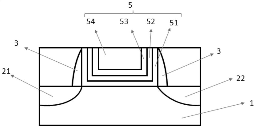
[0032] figure 1 is a schematic structural diagram of the storage unit in Embodiment 1 of the present invention;

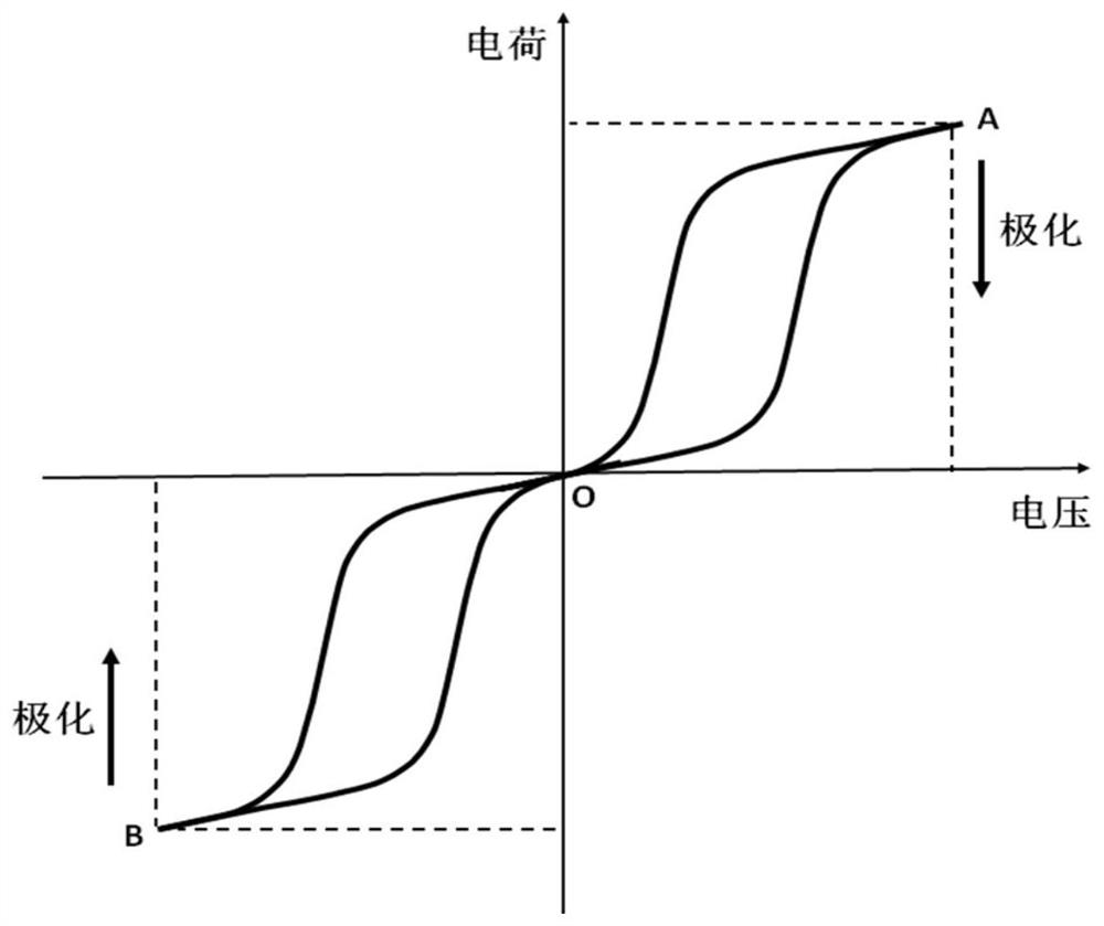
[0033] figure 2 is the polarization charge-voltage curve of the antiferroelectric thin film layer of Example 1 of the present invention.

[0034] Such as figure 1 and 2 As shown, this embodiment provides a memory cell, including: a substrate 1, a source 21 and a drain 22 disposed in the substrate 1, a stacked gate 5 and sidewalls 3; the stacked gate 5 is disposed on The upper surface of the substrate 1 between the source 21 and the drain 22 includes a tunnel oxide layer 51, a charge trapping layer 52, an antiferroelectric thin film layer 53 and a gate electrode 54 arranged sequentially from bottom to top; The gate electrode 54 is used to provide a voltage; the antiferroelectric thin film layer 53 is used to enhance the electric field on the tunnel oxide layer 51 under the action of the voltage, increasing the energy band of the tunnel oxide layer 51 Bending d...

Embodiment 2

[0042] This embodiment provides a method for operating a memory cell. During programming, first apply a positive control voltage on the gate electrode 54, and generate downward polarization in the antiferroelectric thin film layer 53 (control the polarity on the gate electrode 54). Turning the charge to positive corresponds to figure 2 point A in), at this time, a large electric field is generated in the tunneling oxide layer 51, so that the electrons in the substrate 1 tunnel through the tunneling oxide layer 51 to enter and stay in the charge trapping layer 52; then remove the control gate electrode Forward control voltage on 54, the polarization in the antiferroelectric thin film layer will be greatly reduced or reduced to 0, if it is an ideal antiferroelectric thin film, the polarization will be reduced to 0 corresponding figure 2 O point in , while retaining a large number of electrons in the charge trapping layer 52;

[0043] During erasing, a negative control voltage...

Embodiment 3

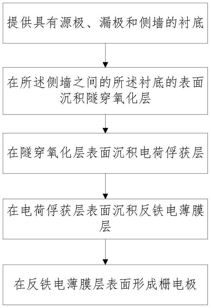
[0045] image 3 It is a flow chart of the manufacturing method of the storage unit according to Embodiment 3 of the present invention; Figure 4 It is a schematic diagram of the manufacturing process of the storage unit according to Embodiment 3 of the present invention.

[0046] Such as image 3 and Figure 4 As shown, the present embodiment provides a method for manufacturing a memory cell, providing a substrate 1 with a source 21, a drain 22 and a spacer 3 (such as Figure 4 a); Deposit a tunnel oxide layer 51 on the surface of the substrate 1 between the sidewalls 3 (such as Figure 4 b); Depositing a charge trapping layer 52 on the surface of the tunnel oxide layer 51 (such as Figure 4 c); Deposit an antiferroelectric film layer 53 on the surface of the charge trapping layer 52 (such as Figure 4 d); form a gate electrode 54 on the surface of the antiferroelectric thin film layer 53 (such as Figure 4 e).

[0047] The memory cell produced by the manufacturing meth...


PUM

PropertyMeasurementUnit
thicknessaaaaaaaaaa

Abstract

The invention relates to a memory cell and an operation method and a preparation method thereof, and the memory cell comprises a substrate, a source electrode and a drain electrode which are arrangedin the substrate, a stacked gate and a side wall. The stacked gate is arranged on the substrate between the source electrode and the drain electrode and comprises a tunneling oxide layer, a charge trapping layer, an anti-ferroelectric film layer and a gate electrode which are sequentially arranged along the direction far away from the substrate. The gate electrode is used for providing a control voltage. The antiferroelectric film layer is used for enhancing an electric field on the tunneling oxide layer under the action of the control voltage and increasing the bending degree of an energy band of the tunneling oxide layer. The charge trapping layer is used for trapping charge storage information injected from the substrate. The storage unit is low in working voltage, high in access speedand low in power consumption.

Description

technical field [0001] The invention relates to the technical field of memory, in particular to a memory unit and its operation method and preparation method. Background technique [0002] Memory is a memory device used to save information in modern information technology. It is one of the basic core components of electronic systems and guarantees the normal operation of the system. For example, all information in a computer, including input raw data, computer programs, intermediate running results, and final running results are stored in memory. [0003] Flash memory (Flash) is a mainstream non-volatile memory at present. However, Flash has the disadvantages of high operating voltage (usually greater than 10V, even 15V) and slow access speed (~1ms), making it difficult to meet the development of future information technology. Contents of the invention [0004] (1) Purpose of the invention [0005] The object of the present invention is to provide a storage unit with lo...

Claims


Application Information

Patent Timeline
Patent Type & Authority Applications(China)
IPC IPC(8): H01L27/11568H01L27/1159
CPCH10B43/30H10B51/30
Inventor 曾斌建周益春廖敏
Owner XIANGTAN UNIV
Why Eureka
Try Eureka