Eureka AIR delivers breakthrough ideas for toughest innovation challenges, trusted by R&D personnel around the world.

High-power semiconductor laser

A semiconductor and laser technology, applied in the field of optical systems, which can solve problems such as the effect of focal depth

Inactive Publication Date: 2020-10-20
深圳活力激光技术有限公司
View PDF3 Cites 1 Cited by
  • Summary
  • Abstract
  • Description
  • Claims
  • Application Information

AI Technical Summary

Problems solved by technology

At present, the laser emitted by the high-power semiconductor laser is a focal point or a focal line after irradiating the surface of the workpiece. Due to the influence of the depth of focus, it has not been possible to realize the zigzag and special-shaped surface of the workpiece in laser processing (the two processing positions on the zigzag and special-shaped surface Different distances from high-power semiconductor lasers)

Method used


Image

  • High-power semiconductor laser
  • High-power semiconductor laser
  • High-power semiconductor laser

Examples


Embodiment Construction

[0037] The application will be further described in detail below with reference to the drawings and embodiments. It is particularly pointed out that the following examples are only used to illustrate the application, but do not limit the scope of the application. Similarly, the following embodiments are only part of the embodiments of the present application, but not all of them. All other embodiments obtained by those of ordinary skill in the art without creative work fall within the protection scope of the present application.

[0038] The terms "first", "second", "third", "fourth", etc. (if any) in the specification and claims of this application and the above-mentioned drawings are used to distinguish similar objects, without having to use To describe a specific order or sequence. It should be understood that the data used in this way can be interchanged under appropriate circumstances, so that the embodiments of the present application described herein, for example, can be ...


PUM

PropertyMeasurementUnit
Angleaaaaaaaaaa

Abstract

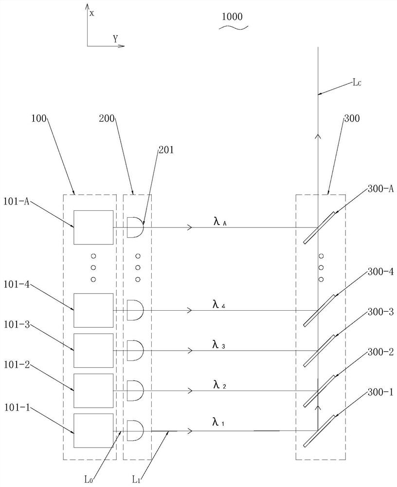
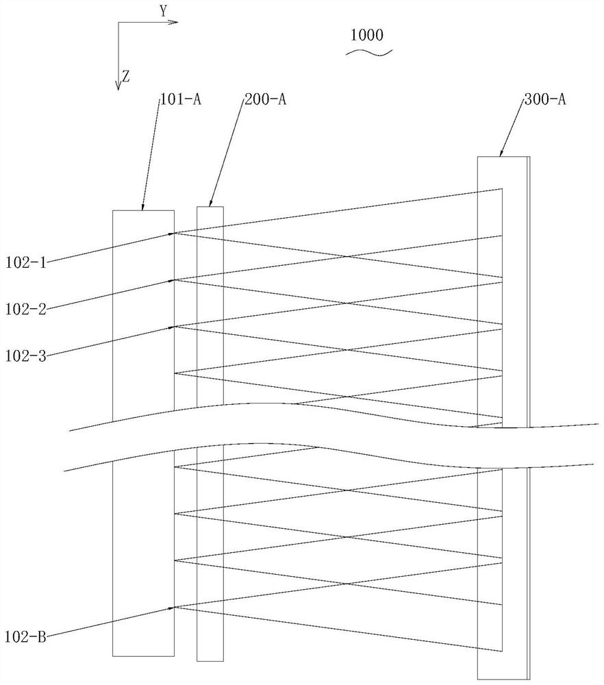
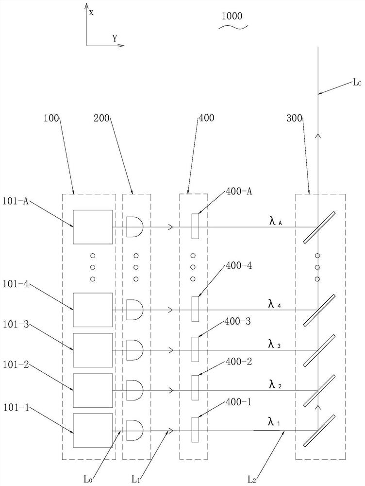
The invention discloses a high-power semiconductor laser, which comprises a laser source, a first optical device and a beam combining device. The laser source comprises a plurality of laser linear arrays, and each laser linear array is provided with a plurality of luminous points. The first optical device collimates the laser beams emitted by the laser source in the fast axis direction, so that the plurality of laser beams emitted by each laser linear array are combined to form a sheet-shaped first laser surface. The beam combining device superposes a plurality of first laser surfaces emittedby the first optical device to form a sheet-shaped superposed laser surface. Laser emitted by the multiple laser linear arrays is superposed through the beam combining device, high-power laser can beoutput, and the device can be used for laser machining, laser engraving and the like. And the light intensity of the superposed laser surface is slightly changed along with the distance between the machined parts, so that the special-shaped surface can be machined, and the long-distance machining can be realized.

Description

Technical field [0001] The invention relates to the technical field of optical systems, in particular to a high-power semiconductor laser. Background technique [0002] Compared with traditional processing methods, laser processing has many significant advantages. When using the laser to process the workpiece, there is no need to contact the workpiece, there is no "tool" wear, the processing speed is fast, the heat impact on the workpiece is small, the processing method is flexible, and it can process a variety of materials with good processing quality. Therefore, laser processing technology is called "the common processing method of the future manufacturing industry." [0003] In recent years, high-power semiconductor lasers have developed rapidly, and their applications in welding and surface treatment have been mature. At present, the laser emitted by a high-power semiconductor laser is a focal point or focus line after irradiating the surface of the workpiece. Affected by the...

Claims


Application Information

Patent Timeline
IPC IPC(8): H01S5/40H01S5/00
CPCH01S5/4025H01S5/4012H01S5/005
Inventor 刘佳敏蔡万绍孙帅
Owner 深圳活力激光技术有限公司
Why Eureka
Eureka Blog
Learn More