Double-layer substrate wiring terminal structure of low-inductance power module
A power module and connection terminal technology, which is applied in the field of low inductance power module double-layer substrate connection terminal structure, can solve the problems of increasing design difficulty and increasing product cost, etc.
- Summary
- Abstract
- Description
- Claims
- Application Information
AI Technical Summary
Problems solved by technology
Method used
Image
Examples
Embodiment Construction
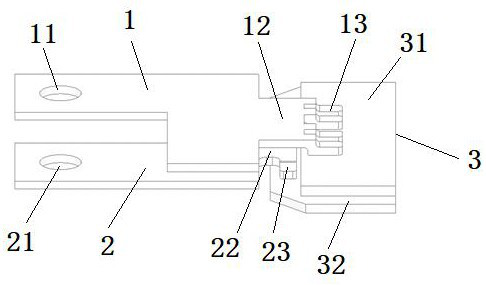
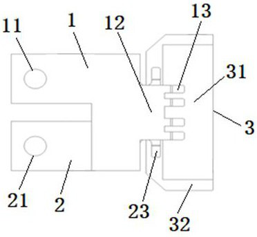
[0027] Example Figure 2 to Figure 5 As shown, the low inductance power module double-layer substrate connection terminal structure of the present invention includes a first connection terminal 1, a second connection terminal 2 and at least one double-layer power module substrate 3, and the first connection terminal 1 and the second connection terminal Some areas of the terminal 2 are overlapped at intervals up and down and form the connection ends 11 and 12 at the front end. parts 13 and 23, the double-layer power module substrate 3 includes a first substrate connection region 31 and a second substrate connection region 32, the connection part 13 of the first connection terminal 1 is connected to the first substrate The area 31 is integrally connected, and the connection portion 23 of the second connection terminal 2 is integrally connected with the second substrate connection area 32 .
[0028] Preferably, the extension portion 12 of the first connection terminal 1 and the ...
PUM
 Abstract
Description
Claims
Application Information


