Supercharge Your Innovation With Domain-Expert AI Agents!

Electronic component detection system and method

一种电子元件、检测系统的技术,应用在检测系统领域,能够解决电子元件无法准确插入电路板、整脚精度不足、插脚偏摆等问题

Pending Publication Date: 2020-10-27
DELTA ELECTRONICS INC
View PDF10 Cites 1 Cited by
  • Summary
  • Abstract
  • Description
  • Claims
  • Application Information

AI Technical Summary

Problems solved by technology

[0003] However, when the scissors are worn out or the precision of the whole pin is insufficient, it may cause abnormal deflection of the pins, resulting in the inability of electronic components to be inserted into the circuit board accurately
Since the pins of electronic components are generally not tested after the automatic whole pin operation, it is impossible to know whether the pins of electronic components are abnormal.

Method used


Image

  • Electronic component detection system and method
  • Electronic component detection system and method
  • Electronic component detection system and method

Examples


Embodiment Construction

[0031] In the various embodiments listed below, the same or similar elements or components will be denoted by the same reference numerals.

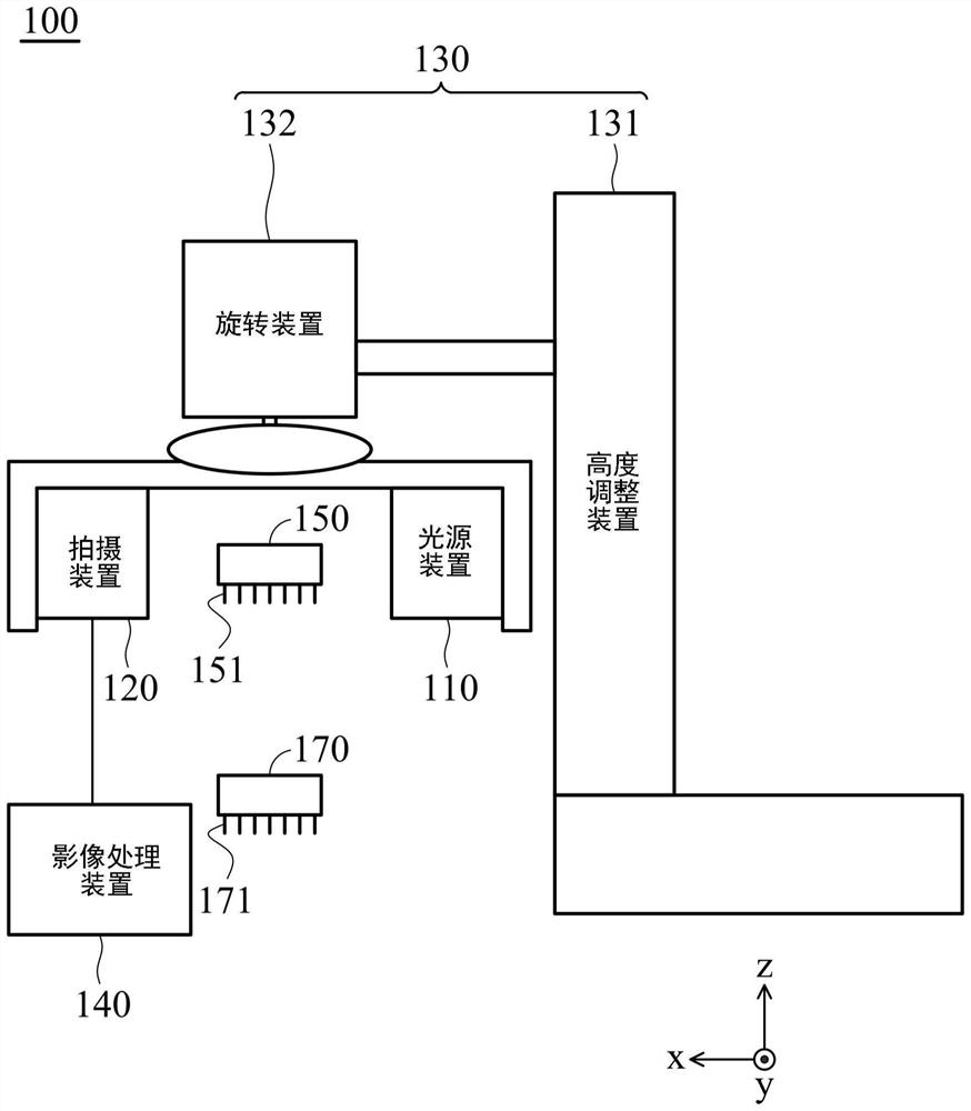
[0032] figure 1 It is a schematic diagram of an electronic component inspection system according to an embodiment of the present invention. Please refer to figure 1 The electronic component inspection system 100 includes a light source device 110 , a camera device 120 , an adjustment device 130 and an image processing device 140 . Note that, figure 1 It is only an embodiment of the present invention, but the present invention is not limited thereto. The electronic component inspection system 100 may also include other components.

[0033] In this embodiment, the light source device 110 , the photographing device 120 , and the adjustment device 130 may be configured on a mobile carrier, and the image processing device 140 may be configured on a machine platform. Wherein, the aforementioned mobile carrier is, for example, a robot arm. ...


PUM


Abstract

An electronic component detection system comprises a light source device, a shooting device, an adjusting device and an image processing device. The light source device generates a light source, and the light source irradiates at least one pin of a first electronic component at different rotation angles. The shooting device senses the light source to generate a plurality of first images and a plurality of second images corresponding to the at least one pin of the first electronic component at different rotation angles. The adjusting device adjusts the shooting device and the light source device to a first height and a second height, the first images correspond to the first height, and the second images correspond to the second height. The image processing device calculates first feature information of the at least one pin of the first electronic component according to the first images and the second images, and analyzes the state of the at least one pin of the first electronic component according to the first feature information. The invention also provides an electronic component detection method.

Description

technical field [0001] The present invention relates to a detection system and method, in particular to an electronic component detection system and method. Background technique [0002] In the traditional printed circuit board (Printed Circuit Board, PCB) manufacturing process, before the electronic components are inserted into the circuit board using the through hole technology (Through Hole Technology, THT), most of the pins of the electronic components need to be adjusted, that is, the pins Cut to length or bent into shape before electronic components can be inserted into the circuit board. [0003] However, when the scissors are worn out or the precision of the whole pin is insufficient, it may cause abnormal deflection of the pins, resulting in the inability of the electronic components to be inserted into the circuit board accurately. Since the pins of the electronic components are generally not tested after the automatic pinning operation, it is impossible to know w...

Claims


Application Information

Patent Timeline
Patent Type & Authority Applications(China)
IPC IPC(8): G01N21/01G01N21/95H05K13/08
CPCG01N21/01G01N21/9515H05K13/08H04N23/80G06T7/0006G06T2207/10016G06T2207/10152G06T2207/30141H05K13/0813H04N23/56H04N23/695H04N23/74H05K13/081G06T7/001
Inventor 黄郁儒黄启铭陈鸿文
Owner DELTA ELECTRONICS INC
Features
  • R&D
  • Intellectual Property
  • Life Sciences
  • Materials
  • Tech Scout
  • Unparalleled Data Quality
  • Higher Quality Content
  • 60% Fewer Hallucinations
Learn More