
Optical detection device and optical detection method thereof

A light detection device and light signal technology, applied in radiation control devices, photovoltaic power generation, semiconductor devices, etc., can solve problems such as performance degradation and leakage current, and achieve the effects of low power consumption, low dark current, and low leakage current

Active Publication Date: 2021-08-03
奥特逻科公司
View PDF7 Cites 0 Cited by
  • Summary
  • Abstract
  • Description
  • Claims
  • Application Information

AI Technical Summary

Problems solved by technology

However, when photodetectors are used in these applications in single or array configurations, leakage currents, dark currents, electrical / optical crosstalk, and power consumption can degrade performance

Method used


Image

  • Optical detection device and optical detection method thereof
  • Optical detection device and optical detection method thereof
  • Optical detection device and optical detection method thereof

Examples


Embodiment Construction

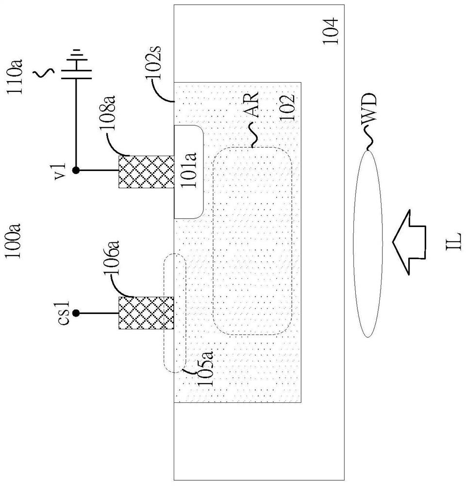
[0027] Figure 1A Illustrated is a cross-sectional view of a light detection device according to some embodiments. The photodetection device 100 a includes a germanium-based light-absorbing material 102 supported by a semiconductor substrate 104 . In one implementation, the semiconductor substrate 104 is made of silicon or silicon germanium or germanium or III-V compounds. The germanium-based light-absorbing material 102 refers herein to intrinsic germanium (100% germanium) or an alloy of elements including germanium, such as a silicon-germanium alloy with a Ge concentration of 1% to 99%. In some implementations, germanium-based light absorbing material 102 can be grown using blanket epitaxy, selective epitaxy, or other suitable techniques. Ge-based light absorbing material 102 is embedded in the Figure 1A In the semiconductor substrate 104 , in alternative embodiments, the germanium-based light absorbing material 102 may be partially embedded in the semiconductor substrat...


PUM

PropertyMeasurementUnit
wavelengthaaaaaaaaaa

Abstract

A photodetection device includes a semiconductor substrate. A first germanium-based light absorbing material is supported by the semiconductor substrate and configured to absorb a first light signal having a first wavelength greater than 800 nm. A first metal line is electrically coupled to the first region of the first germanium-based light absorbing material. A second metal line is electrically coupled to the second region of the first germanium-based light absorbing material. The first region is undoped or doped with a dopant of the first type. The second region is doped with a second type of dopant. The first metal line is configured to control the amount of photogenerated carriers of the first type generated inside the first germanium-based light absorbing material to be collected by the second region.

Description

[0001] Cross References to Related Applications [0002] This patent application claims the benefit of: U.S. Provisional Patent Application No. 62 / 634,741, filed February 23, 2018, U.S. Provisional Patent Application No. 62 / 654,454, filed April 8, 2018, April 20, 2018 U.S. Provisional Patent Application No. 62 / 660,252, filed July 15, 2018, U.S. Provisional Patent Application No. 62 / 698,263, filed June 8, 2018, U.S. Provisional Patent Application No. 62 / 682,254, filed June 8, 2018, June 19, 2018 U.S. Provisional Patent Application No. 62 / 686,697 filed on July 8, 2018, U.S. Provisional Patent Application No. 62 / 695,060 filed on July 8, 2018, U.S. Provisional Patent Application No. 62 / 695,058 filed on July 8, 2018, October 2018 U.S. Provisional Patent Application No. 62 / 752,285 filed on August 29, U.S. Provisional Patent Application No. 62 / 717,908 filed on August 13, 2018, U.S. Provisional Patent Application No. 62 / 755,581 filed on November 5, 2018, U.S. Provisional Patent Applica...

Claims


Application Information

Patent Timeline
Patent Type & Authority Patents(China)
IPC IPC(8): H01L27/144H01L27/148
CPCH01L27/14806H01L27/14831H01L31/103H01L31/035272H01L31/108Y02E10/50H01L31/02024H01L31/035254H01L31/0284H01L27/15H01L31/1812H01L31/1075H01L31/0745
Inventor 陈书履陈建宇郑斯璘那允中杨闵杰刘汉鼎梁哲夫
Owner 奥特逻科公司
Features
  • Generate Ideas
  • Intellectual Property
  • Life Sciences
  • Materials
  • Tech Scout
  • Unparalleled Data Quality
  • Higher Quality Content
  • 60% Fewer Hallucinations
Learn More