An IGBT device with latch-up resistance

A technology of anti-latch-up and ability, applied in the direction of semiconductor devices, electrical components, circuits, etc., can solve problems such as threshold voltage influence, device failure, and increased difficulty of P-plus, so as to achieve low equipment requirements, suppress pnpn latch-up, and improve The effect of short-circuit capability and latch-up immunity

Pending Publication Date: 2020-11-03
南京晟芯半导体有限公司
View PDF0 Cites 0 Cited by
  • Summary
  • Abstract
  • Description
  • Claims
  • Application Information

AI Technical Summary

Problems solved by technology

[0003] Compared with N-channel MOSFETs, N-channel IGBTs have an extra layer of P-type collectors on the back, so there is a parasitic pnpn structure in the vertical direction. In the early stage, in order to prevent the parasitic pnpn from forming a latch and causing device failure, the prior art usually Use the source contact hole to short-circuit the N-type source region and the P-type body region and add a P-type implant between the trench gate. However, as the equipment capacity increases year by year, the number of cells per unit area of ​​the IGBT device gradually increases, and the trench gate The mesa area between is also getting narrower, making it more difficult to align the P-plus implantation, and as the mesa area becomes narrower, the P-plus implantation will have a serious impact on parameters such as threshold voltage

Method used


Image

  • An IGBT device with latch-up resistance
  • An IGBT device with latch-up resistance
  • An IGBT device with latch-up resistance

Examples


Embodiment 1

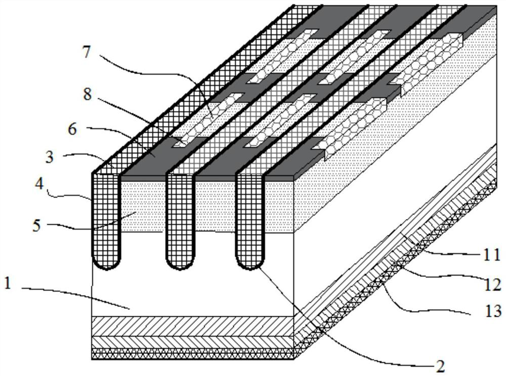
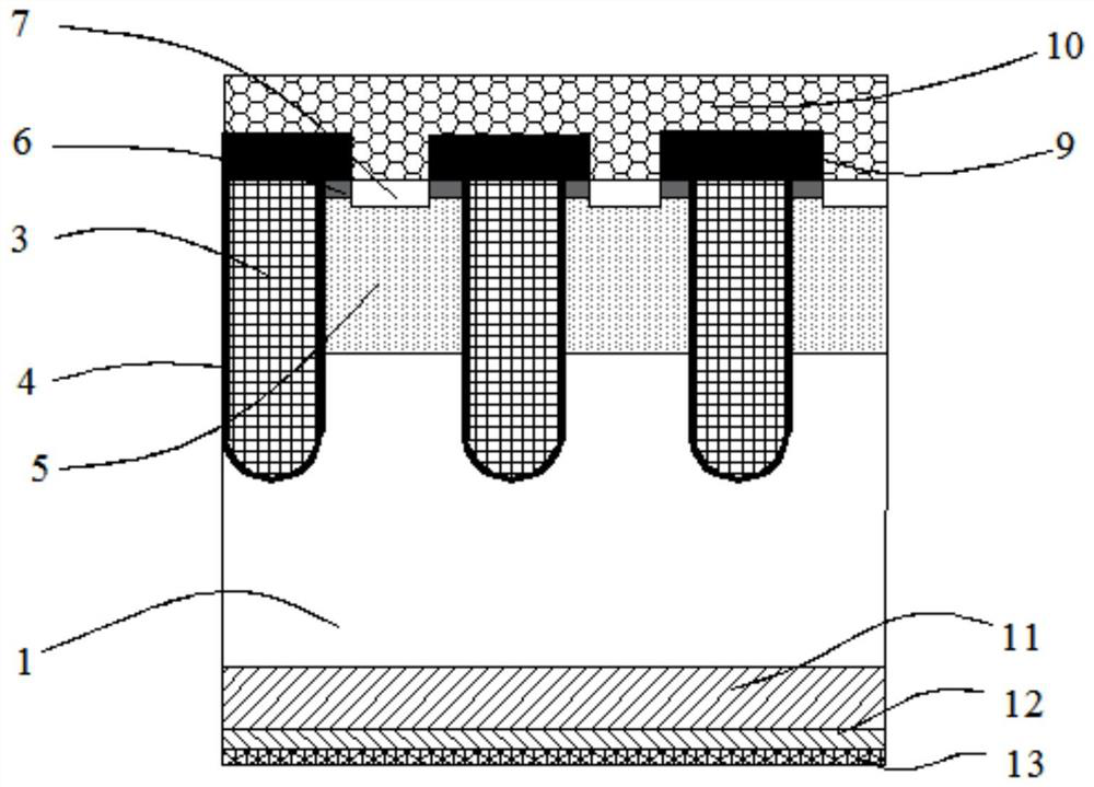
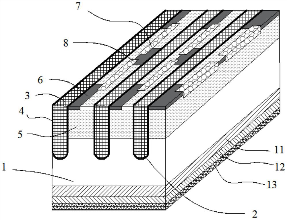
[0027] This embodiment provides an IGBT device structure, please refer to figure 1 and image 3 , which are respectively shown as a perspective view and a cross-sectional view of the IGBT device structure. As shown in the figure, the IGBT device structure includes:

[0028] The segmented N-type source region 6 and the segmented source region contact hole region 7, the N-type source region 6 and the source region contact hole region 7 have an overlapping area 8, the size of the overlapping area 8 is adjustable, and is used to control the introduced The size of the ballast resistor.

[0029] An N-type drift region 1 is set below the P-type body region 5, and a number of trench gates 2 are arranged above the N-type drift region 1. Between the trench gates 2 is a P-type body region 5, and the lower boundary of the P-type body region 5 higher than the bottom of the trench gate 2; the segmented N-type source region 6 is located between the trench gates 3 and embedded above the P-t...

Embodiment 2

[0037] This embodiment adopts basically the same technical solution as Embodiment 1, except that in Embodiment 1, the width of the N-type source region 6 fills up the width of two adjacent trench gates 2; The segmented N-type source region 6 between the trench gates 2 is only in contact with the trench gate 2 on one side, that is, the width of the N-type source region 6 does not fill up two adjacent trench gates 2; Two adjacent segmented N-type source regions 6 between two trench gates 2 are in contact with trench gates 2 on different sides. In Embodiment 1, the length of the overlapping region 8 of the source contact hole region 7 and the N-type source region 6 is 1 μm, while in this embodiment, the length of the overlapping region 8 of the source contact hole region 7 and the N-type source region 6 The length is 2 μm.

[0038] see figure 2 , which is a perspective view of the structure of the IGBT device in this embodiment, as shown in the figure, the length of the overla...


PUM

PropertyMeasurementUnit
Lengthaaaaaaaaaa
Lengthaaaaaaaaaa

Abstract

The invention relates to an IGBT device with latch-up resistance, and belongs to the technical field of power semiconductor devices. According to the invention, a sectional type N-type source region and a sectional type source region contact hole region are used, and the size of the introduced ballast resistance is controlled by adjusting the size of the overlapped region of the N-type source region and the source region contact hole, so that the potential of the N-type source region during conduction is controlled, and the purpose of latch-up resistance is achieved. According to the structurefor reducing the latch-up risk of the IGBT device, a method for providing ballast resistance by controlling a circulation path of electrons is adopted, the process is simple, the equipment requirement is low, P-type injection does not need to be additionally introduced, latch-up can be effectively restrained, and meanwhile the short-circuit capacity is improved.

Description

technical field [0001] The invention belongs to the technical field of IGBT devices and relates to an IGBT device with anti-latch capability. Background technique [0002] IGBT (Insulated Gate Bipolar Transistor) is a composite fully-controlled voltage-driven power semiconductor device composed of bipolar transistors and MOSFETs. It also has high input impedance of MOSFETs and low conduction voltage drop of GTR. At this stage, IGBT has become the mainstream device of power electronic equipment, and has a wide range of applications in switching power supplies, rectifiers, inverters, UPS and other fields. [0003] Compared with N-channel MOSFETs, N-channel IGBTs have an extra layer of P-type collectors on the back, so there is a parasitic pnpn structure in the vertical direction. In the early stage, in order to prevent the parasitic pnpn from forming a latch and causing device failure, the prior art usually Use the source contact hole to short-circuit the N-type source region...

Claims


Application Information

Patent Timeline
IPC IPC(8): H01L29/739H01L29/06
CPCH01L29/0603H01L29/0684H01L29/0696H01L29/7397
Inventor 许海东
Owner 南京晟芯半导体有限公司
Why Eureka
Try Eureka