Negative feedback type single photon avalanche photodiode and manufacturing method thereof

A single-photon avalanche and photodiode technology, applied in circuits, electrical components, semiconductor devices, etc., can solve problems such as quenching time and long recovery time, and achieve the goals of reducing avalanche time, fast recovery, and improving quenching and recovery time Effect

Pending Publication Date: 2020-11-10
THE 44TH INST OF CHINA ELECTRONICS TECH GROUP CORP
View PDF8 Cites 3 Cited by
  • Summary
  • Abstract
  • Description
  • Claims
  • Application Information

AI Technical Summary

Problems solved by technology

[0007] In order to solve the problem of long quenching time and recovery time affected by parasitic parameters in passive quenching mode, the present invention provides a negative feedback single photon avalanche photodiode and its manufacturing method

Method used


Image

  • Negative feedback type single photon avalanche photodiode and manufacturing method thereof
  • Negative feedback type single photon avalanche photodiode and manufacturing method thereof
  • Negative feedback type single photon avalanche photodiode and manufacturing method thereof

Examples


Embodiment Construction

[0039] The following will clearly and completely describe the technical solutions in the embodiments of the present invention with reference to the accompanying drawings in the embodiments of the present invention. Obviously, the described embodiments are only some of the embodiments of the present invention, not all of them. Based on the embodiments of the present invention, all other embodiments obtained by persons of ordinary skill in the art without making creative efforts belong to the protection scope of the present invention.

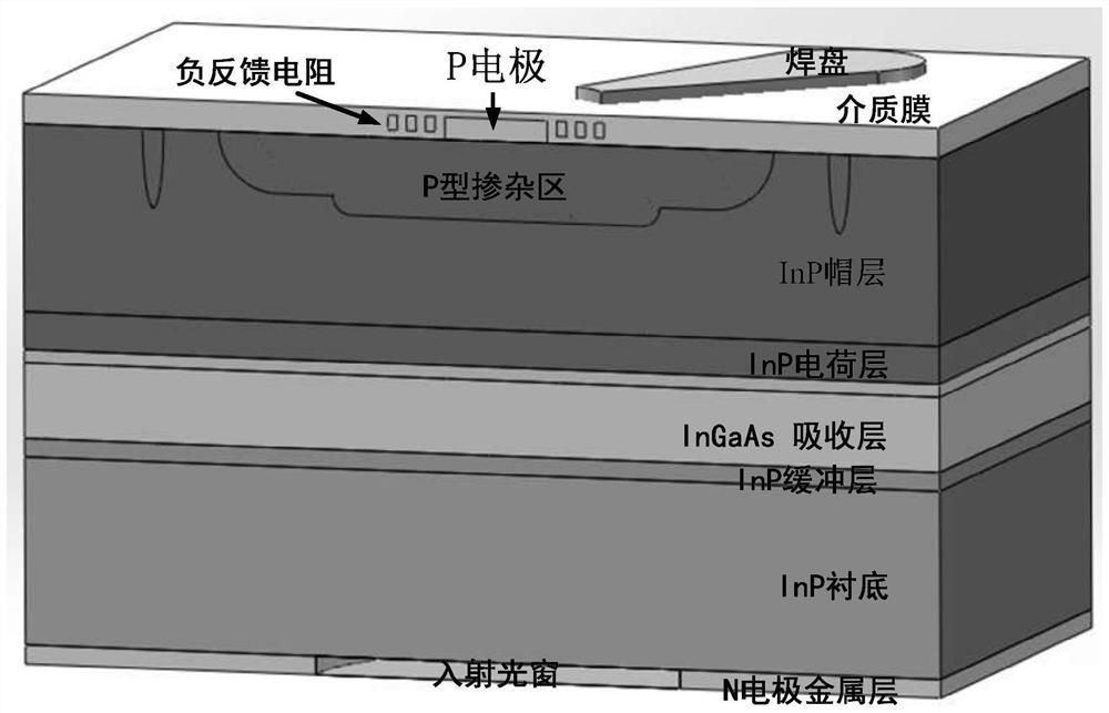
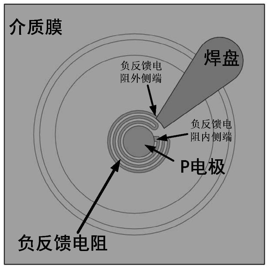
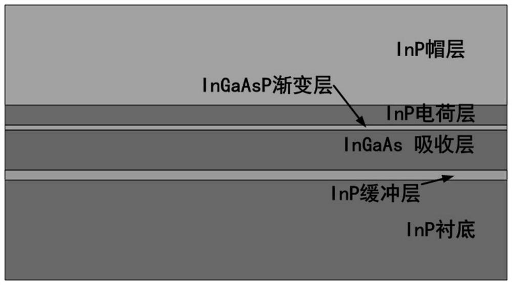
[0040] Figure 1-2It is a schematic diagram of the NFAD structure of the present invention, a negative feedback type single-photon avalanche photodiode, including: a substrate, a buffer layer, an absorption layer, a gradient layer, a charge layer and a cap layer, and an incident light window and a cap layer are arranged below the substrate. N electrodes, and the N electrodes are symmetrically arranged around the incident light window; a buffer la...


PUM

PropertyMeasurementUnit
thicknessaaaaaaaaaa
electrical resistivityaaaaaaaaaa

Abstract

The invention relates to the technical field of semiconductor photoelectrons, in particular to a negative feedback type single photon avalanche photodiode and a manufacturing method thereof. The negative feedback type single photon avalanche photodiode comprises a substrate, a buffer layer, an absorption layer, a gradient layer, a charge layer and a cap layer, wherein an incident light window andN electrodes are arranged below the substrate, and the N electrodes are symmetrically distributed around the incident light window; the buffer layer, the absorption layer, the gradient layer, the charge layer and the cap layer are sequentially arranged above the substrate; a P-type doped region with a stepped structure is arranged on the cap layer, and a P electrode grows on the P-type doped region; a dielectric film is arranged on the upper surface of the cap layer, a negative feedback resistor of a semi-closed convolution annular structure is arranged in the middle of the dielectric film, abonding pad is arranged on the dielectric film, one end of the negative feedback resistor is connected with the P electrode, and the other end is connected with the bonding pad. Rapid quenching and rapid recovery of single photon avalanche photodiode SPAD Geiger avalanche can be realized so that the photon detection rate of the SPAD can be enhanced, the post-pulse effect can be reduced and the photon detection function of unpredictable arrival time can be realized.

Description

technical field [0001] The invention relates to the technical field of semiconductor optoelectronics, in particular to a negative feedback type single photon avalanche photodiode and a manufacturing method thereof. Background technique [0002] With the continuous development of technologies such as quantum secure communication, single-photon detection, and laser ranging, single-photon detectors have been rapidly developed and widely used. A single photon avalanche photodiode (Single Photon Avalanche Diode, SPAD) is used for the detection of photon signals and is one of the core chips of a single photon detector. [0003] In order to realize single-photon detection, the SPAD based on the Separate Absorption Charge Multiplication (SACM) structure must work in the Geiger mode, that is, the voltage across the SPAD is above its avalanche voltage. In the Geiger mode, the photon signal detected by the SPAD outputs a macroscopically detectable electrical signal, but if it continue...

Claims


Application Information

Patent Timeline
Patent Type & Authority Applications(China)
IPC IPC(8): H01L31/107H01L31/18
CPCH01L31/107H01L31/184
Inventor 陈伟高新江赵江林刘昆敖天宏蒋利群罗洪静张承陈扬黄晓峰
Owner THE 44TH INST OF CHINA ELECTRONICS TECH GROUP CORP
Why Eureka
Try Eureka