Transistor groove manufacturing method and transistor

A manufacturing method and transistor technology, applied in semiconductor/solid-state device manufacturing, semiconductor devices, nanotechnology for information processing, etc., can solve problems such as roughness and the introduction of impurities on the surface, and achieve the effect of reducing the surface state density

Active Publication Date: 2020-11-17
深圳市红与蓝企业管理中心(有限合伙)
View PDF5 Cites 1 Cited by
  • Summary
  • Abstract
  • Description
  • Claims
  • Application Information

AI Technical Summary

Problems solved by technology

However, the enhancement mode HEMT device based on the etching method will introduce impurities on the surface of the groove and cause the surface roughness during etching or photolithography, thereby introducing high-density surface states

Method used


Image

  • Transistor groove manufacturing method and transistor
  • Transistor groove manufacturing method and transistor
  • Transistor groove manufacturing method and transistor

Examples


Embodiment Construction

[0039] The following will clearly and completely describe the technical solutions in the embodiments of the present invention with reference to the accompanying drawings in the embodiments of the present invention. Obviously, the described embodiments are some of the embodiments of the present invention, but not all of them. Based on the embodiments of the present invention, all other embodiments obtained by persons of ordinary skill in the art without creative efforts fall within the protection scope of the present invention.

[0040] In the description of the present invention, it should be noted that the terms "first", "second", "third" and so on are only used to distinguish descriptions, and should not be understood as indicating or implying relative importance.

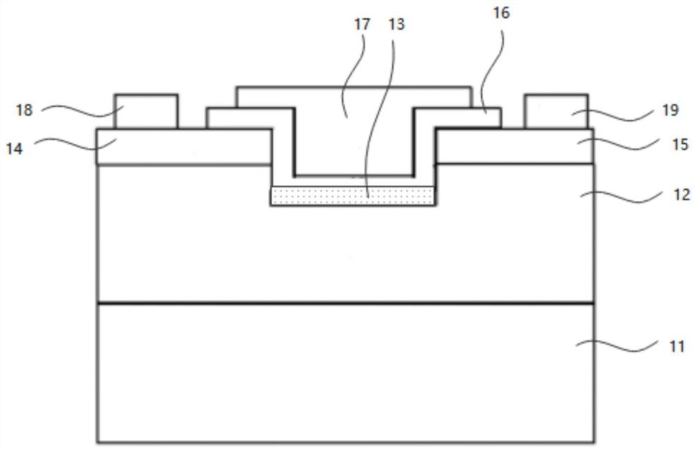
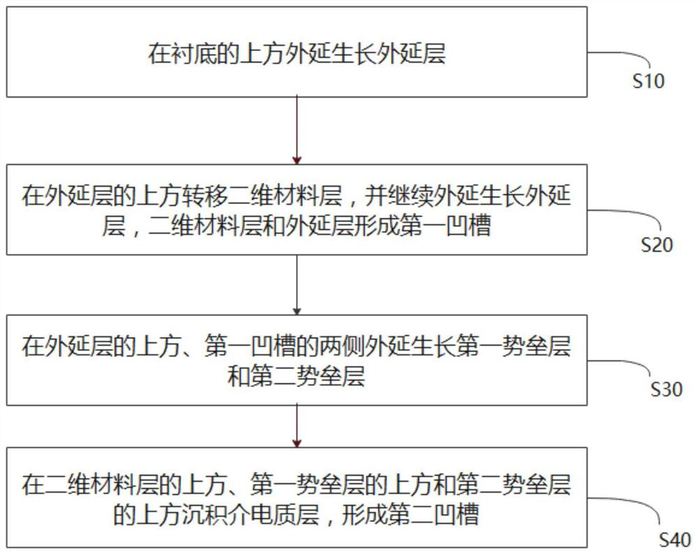
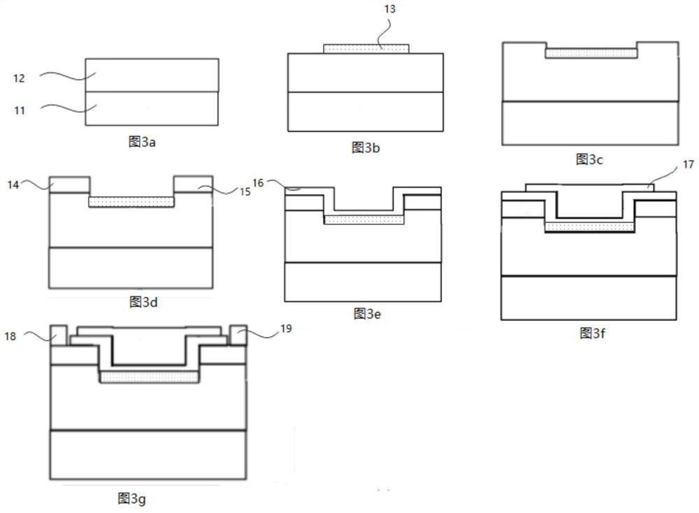
[0041] Embodiments of the present invention provide a method for manufacturing grooves of transistors, which can be used for manufacturing such as figure 1 The transistor shown, the transistor may be a high elect...


PUM

PropertyMeasurementUnit
thicknessaaaaaaaaaa
thicknessaaaaaaaaaa
thicknessaaaaaaaaaa

Abstract

The invention provides a transistor groove manufacturing method and a transistor. The method comprises the following steps: epitaxially growing an epitaxial layer above a substrate; transferring the two-dimensional material layer above the epitaxial layer, continuing to epitaxially grow the epitaxial layer, and forming a first groove by the two-dimensional material layer and the epitaxial layer; epitaxially growing a first barrier layer and a second barrier layer above the epitaxial layer and on two sides of the first groove; and depositing a dielectric layer above the two-dimensional materiallayer, the first barrier layer and the second barrier layer to form a second groove. According to the groove system of the transistor manufactured through the method, the surface of the groove is smoother, and the surface state density is lower.

Description

technical field [0001] The invention relates to the field of semiconductors, in particular to a method for manufacturing a transistor groove and the transistor. Background technique [0002] High Electron Mobility Transistor (HEMT) is widely used in various fields. Since a two-dimensional electron gas is formed at the heterojunction interface between GaN and AlGaN, the two-dimensional electron gas has extremely high carrier concentration and carrier mobility, so GaN and AlGaN are ideal materials for preparing HEMT devices. However, since the depletion-mode HEMT device is a normally-on device, a large amount of additional energy will be lost when the depletion-mode HEMT device is used for operation. The enhanced HEMT device does not have the above problems. The conventional enhancement mode HEMT device is based on the depletion mode HEMT device, using an etching method to etch a groove structure at the gate of the HEMT device to interrupt the transmission of the two-dimensi...

Claims


Application Information

Patent Timeline
Patent Type & Authority Applications(China)
IPC IPC(8): H01L21/335H01L29/778B82Y40/00B82Y10/00
CPCH01L29/7781H01L29/66462B82Y10/00B82Y40/00Y02P70/50
Inventor 刘新科贲建伟利健罗江流王磊贺威林峰黎晓华朱德亮吕有明
Owner 深圳市红与蓝企业管理中心(有限合伙)
Why Eureka
Try Eureka