Solar cell, front film layer structure of solar cell, preparation method of front film layer structure, assembly and system

A technology of solar cells and film layer structure, applied in the field of solar cells, can solve the problems of poor anti-PID potential induction performance and low conversion efficiency of battery components, and achieves improved compactness and passivation effect, increased absorption and utilization, and increased light. absorption effect

Pending Publication Date: 2022-01-11
TIANJIN AIKO SOLAR ENERGY TECH CO LTD +3
View PDF0 Cites 0 Cited by
  • Summary
  • Abstract
  • Description
  • Claims
  • Application Information

AI Technical Summary

Problems solved by technology

[0003] The purpose of the embodiments of the present invention is to provide a front film structure of a solar cell, which aims to solve the problems of low conversion efficiency of the battery in the existing front film structure and poor anti-PID potential induction performance of the battery module

Method used


Image

  • Solar cell, front film layer structure of solar cell, preparation method of front film layer structure, assembly and system
  • Solar cell, front film layer structure of solar cell, preparation method of front film layer structure, assembly and system

Examples


Embodiment 1

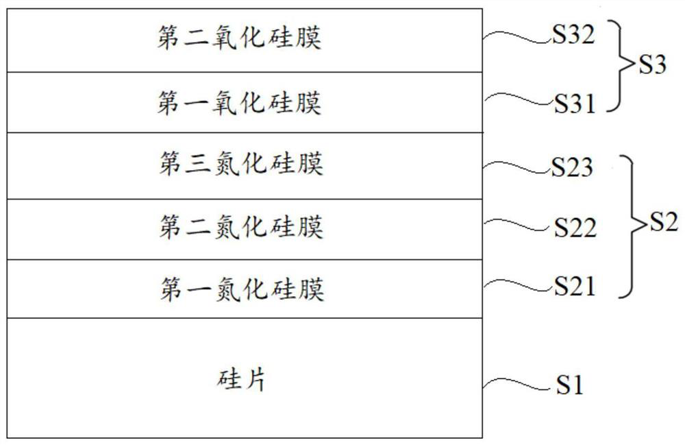
[0052] see figure 1 , is a structural schematic diagram of the front film layer structure of the solar cell provided by the first embodiment of the present invention. For the convenience of description, only the parts related to the embodiment of the present invention are shown. The front film layer of the solar cell provided by the embodiment of the present invention The structure includes a silicon nitride layer S2 and a silicon oxide layer S3 sequentially deposited on the front side of the silicon wafer S1;

[0053] The silicon nitride layer S2 is composed of at least three layers of silicon nitride films with different refractive indices; the silicon oxide layer S3 is composed of at least two layers of silicon oxide films with different refractive indices.

[0054] The refractive index of each layer of silicon nitride film and silicon oxide film arranged in sequence decreases successively.

[0055] Among them, in one embodiment of the present invention, the front film lay...

Embodiment 2

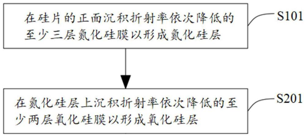
[0070] see figure 2 , is a schematic flow chart of a method for preparing a solar cell front film structure provided by the second embodiment of the present invention. For the convenience of description, only the parts related to the embodiment of the present invention are shown. The front film layer structure of the solar cell of the embodiment, specifically, the method includes:

[0071] Step S11, depositing a silicon nitride layer S2 on the front surface of the silicon wafer S1; depositing at least three layers of silicon nitride films with a gradually decreasing refractive index on the front surface of the silicon wafer to form a silicon nitride S2 composed of multiple layers of silicon nitride films layer;

[0072] Among them, in the embodiment of the present invention, a single crystal silicon wafer is selected, which is processed into a silicon substrate required for deposition after sequential texturing, diffusion, SE laser, etching, and annealing treatments, specifi...

Embodiment 3

[0105] The third embodiment of the present invention also provides a solar cell, which includes a silicon wafer, a back film structure deposited on the back of the silicon wafer, and a front film structure as in the preceding embodiment deposited on the front of the silicon wafer.

[0106] This embodiment provides a solar cell with high performance and high reliability. By setting at least three silicon nitride layers and at least two silicon oxide film layers in the front film system, compared with the existing front film structure, A layer of silicon nitride film and silicon oxide film is added to increase the absorption of short-wavelength light and reduce the reflection of light back to the incident interface to reduce the reflection loss of light on the front side, thereby increasing the absorption and utilization of light by silicon wafers and improving solar cells. The conversion efficiency of the front side is increased by more than 0.05%; through the cooperation of at ...


PUM

PropertyMeasurementUnit
thicknessaaaaaaaaaa
thicknessaaaaaaaaaa
thicknessaaaaaaaaaa

Abstract

The invention is suitable for the technical field of solar cells, and provides a solar cell, a front film layer structure of the solar cell, a preparation method of the front film layer structure, an assembly and a system. According to the solar cell front film layer structure provided by the embodiment of the invention, at least three silicon nitride layers and at least two silicon oxide film layers are arranged in the front film layer; compared with an existing front surface film layer structure, light absorption of short wavelength is increased, light reflection back to an incident interface is reduced, reflection loss of light on the front surface is reduced, light absorption and utilization of a silicon wafer are increased, the conversion efficiency of the front surface of the solar cell is improved, and the efficiency of the front surface is improved by more than 0.05%; compared with the prior art, the invention has the advantages of improving the contact with the silicon wafer, improving the compactness and passivation effect of the front surface of the battery, effectively reducing the state density of the silicon surface and reducing the non-radiative recombination of carriers, thereby effectively improving the potential induced degradation resistance of the battery assembly, delaying the attenuation of the battery assembly and prolonging the service life of the battery assembly.

Description

technical field [0001] The invention belongs to the field of solar cells, and in particular relates to a solar cell and its front film layer structure as well as a preparation method, component and system thereof. Background technique [0002] The front film structure of the existing P-type or N-type crystalline silicon solar cells adopts a film structure of two layers of silicon nitride superimposed on a layer of silicon oxide. It is found that the existing front film structure of two layers of silicon nitride anti-reflection The effect is poor, resulting in a low conversion rate of the front membrane battery. In addition, the existing front film structure is poor in compactness, resulting in poor water vapor resistance. In the case of high temperature and humidity, water vapor enters the battery components, causing the acetic acid produced by the hydrolysis of EVA (vinyl acetate) to react with the component glass to form Na+, Ca+ , Fe+, etc. Alkali ions form a leakage cur...

Claims


Application Information

Patent Timeline
Patent Type & Authority Applications(China)
IPC IPC(8): H01L31/0216H01L31/18
CPCH01L31/02168H01L31/02167H01L31/1868H01L31/1804Y02E10/547Y02P70/50
Inventor 赵小平陈刚
Owner TIANJIN AIKO SOLAR ENERGY TECH CO LTD
Why Eureka
Try Eureka