Method for growth and preparation of III-nitride Schottky barrier diode

A Schottky potential, nitride technology, applied in semiconductor/solid-state device manufacturing, electrical components, circuits, etc., can solve problems such as reducing the performance of Schottky diodes, achieve simple structure, low reverse leakage current, and improve resistance The effect of pressure characteristics

Inactive Publication Date: 2015-07-22
SUN YAT SEN UNIV
View PDF6 Cites 0 Cited by
  • Summary
  • Abstract
  • Description
  • Claims
  • Application Information

AI Technical Summary

Problems solved by technology

[0005] However, the electrical characteristics of Schottky barrier diodes have a lot to do with the properties of the semiconductor material itself. Due to the influence of lattice mismatch and thermal mismatch, the existence of heteroepitaxial III-nitride-based materials is inevitable. Higher density of defects, these defects make the Group-III nitride-based Schottky barrier diodes inevitably introduce leakage channels during the fabrication process, which greatly reduces the performance of Schottky diodes

Method used


Image

  • Method for growth and preparation of III-nitride Schottky barrier diode
  • Method for growth and preparation of III-nitride Schottky barrier diode
  • Method for growth and preparation of III-nitride Schottky barrier diode

Examples


Embodiment 1

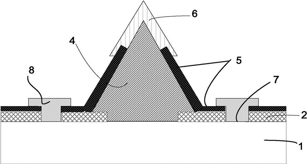
[0036] attached figure 1It is a schematic diagram of the design of Embodiment 1, which combines vertical and horizontal conductive structures. The basic structure includes: substrate 1 , mask layer 2 , selective growth window 3 , epitaxially grown III-nitride three-dimensional structure 4 , barrier layer 5 , Schottky contact layer 6 , and ohmic contact layer 7 . Combine below Figure 2a -2e describes the manufacturing process of embodiment 1 in detail.

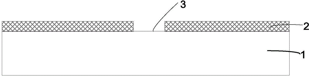
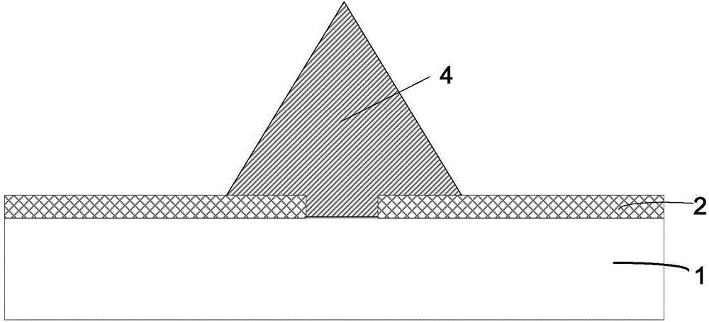
[0037] see Figure 2a , provide an underlying substrate 1, the material of the underlying substrate 1 can be Si, GaN, ZnO, AlN, AlGaN, Al 2 o 3 , diamond, SiC and other bulk materials, and a composite substrate material formed of a single-layer or multi-layer III-nitride material or ZnO material grown on the above-mentioned bulk material substrate can also be selected. A mask layer 2 is then deposited on the substrate 1 . The material of the mask layer 2 can be selected from high-resistance materials such as SiO2, SiN, A...

Embodiment 2

[0044] as attached Figure 6 As shown, it is a cross-sectional view of another III-nitride Schottky barrier diode combining vertical and lateral conductive structures of the present invention. The structure in this embodiment is basically the same as that in Embodiment 1, except that the metal layer of the Schottky contact layer 6 extends to the top of the entire three-dimensional structure 4 and overlaps with the barrier layer 5 . The advantage of embodiment 2 compared with embodiment 1 is that embodiment 2 has a field plate structure, which effectively avoids the edge effect of current and is conducive to conduction of a larger forward current. FIG. 7 is a perspective view of a group-III nitride Schottky barrier diode with a hexagonal pyramid structure prepared based on Example 2. FIG.

Embodiment 3

[0046] as attached Figure 8 Shown is Embodiment 3 of the present invention, a cross-sectional view of a group-III nitride Schottky barrier diode with a vertical conduction structure. The structure in this embodiment is basically the same as that in Embodiment 1, except that the ohmic contact layer 8 is located on the back of the substrate 1 and forms a good ohmic contact with the substrate 1 . Embodiment 3 does not need to etch the through-hole structure 7, the process is relatively simple, and the Schottky contact layer and the ohmic contact layer of the structure are located on the upper and lower surfaces of the device, so that the device has vertical conduction characteristics and avoids current edge collection effect, it is convenient to realize parallel packaging of multiple devices. Accompanying drawing 9 is the perspective view of a group-III nitride Schottky barrier diode with a strip-shaped three-dimensional structure prepared based on Example 3.


PUM


Abstract

The invention discloses a method for preparing a III-nitride Schottky barrier diode (SBD) which is provided with a thick film and is low in defect density and high in pressure resistance. A method of selection region epitaxial growth is utilized for the III-nitride SBD. The III-nitride SBD structurally sequentially comprises a bottom layer substrate, a dielectric layer, a III-nitride three-dimensional structure, a side wall barrier layer, a Schottky contact layer and an Ohmic contact layer from bottom to top, wherein the dielectric layer is provided with a selection region growth window; the III-nitride three-dimensional structure is obtained by utilizing the selective epitaxial growth; and the side wall barrier layer is used for preventing electric leakage. The three-dimensional III-nitride structure obtained through the selective epitaxial growth method is large in thickness and lower in defect density, the SBD has a lower reverse leakage current and higher reverse breakdown voltage; the III-nitride SBD is simple in structure, the parallel connection packaging of multiple devices is achieved easily, and the method has wide prospect in the aspect of high-current high-voltage resistant SBD devices.

Description

technical field [0001] The invention relates to the field of semiconductor device manufacturing, in particular to a method for manufacturing a Schottky barrier diode device based on a three-dimensional structure of a low-defect density group III nitride. Background technique [0002] After half a century of development, the semiconductor industry has experienced the first generation of silicon (Si) and germanium (Ge) element semiconductor materials, the second generation of gallium arsenide (GaAs), and indium phosphide (InP) compound semiconductor materials, and has entered the first generation. The era of three generations of wide bandgap semiconductor materials. As a typical representative of the third-generation semiconductor materials, III-nitride materials (including indium nitride, gallium nitride, aluminum nitride and their multi-component alloys) have excellent physical and electrical properties. Compared with most of the current semiconductor materials, III-nitride...

Claims


Application Information

Patent Timeline
Patent Type & Authority Applications(China)
IPC IPC(8): H01L21/329H01L29/872
CPCH01L29/66143H01L29/0684H01L29/2003H01L29/401
Inventor 张佰君陈杰刘扬
Owner SUN YAT SEN UNIV
Why Eureka
Try Eureka