Manufacture method of table surface type indium gallium arsenic detector

A detector, indium gallium arsenide technology, used in semiconductor devices, final product manufacturing, sustainable manufacturing/processing, etc., can solve problems such as passivation film damage and failure, achieve lattice repair, reduce surface fixed charge, reduce The effect of lattice damage

Active Publication Date: 2013-05-29
SHANGHAI INST OF TECHNICAL PHYSICS - CHINESE ACAD OF SCI
View PDF1 Cites 0 Cited by
  • Summary
  • Abstract
  • Description
  • Claims
  • Application Information

AI Technical Summary

Problems solved by technology

[0009] Based on the problems existing in the preparation process of the above-mentioned mesa detectors, the purpose of the present invention is to provide a method for preparing a mesa-type indium gallium arsenide (InGaAs) detector chip, to solve the problem of passivation film damage and failure caused by annealing, and to improve the long-term The uniformity and yield of the column and area array detectors, in addition, by introducing heat treatment, chemical corrosion to remove surface oxides and surface sulfide processes, effectively reduce the surface state density introduced by ion etching, and improve the detection efficiency of the detector. Dark current performance

Method used


Image

  • Manufacture method of table surface type indium gallium arsenic detector
  • Manufacture method of table surface type indium gallium arsenic detector

Examples


Embodiment Construction

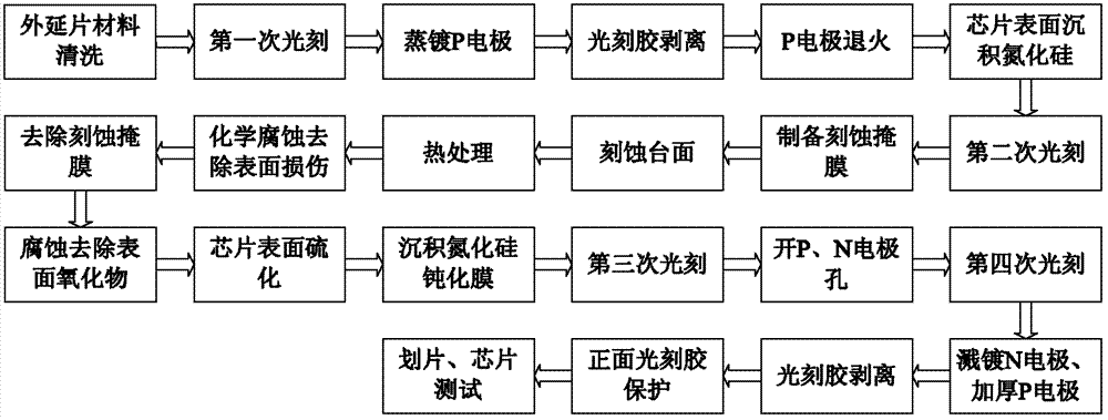
[0047] The specific implementation method of the present invention will be described in detail below.

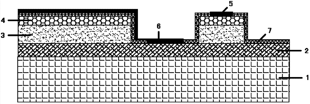
[0048] as attached figure 2 As shown, the epitaxial wafer used in the detector of this embodiment is an N-type InP layer 2 with a thickness of 1.5 μm grown sequentially on a semi-insulating InP substrate 1 with a thickness of 350 μm by gas source molecular beam epitaxy (GSMBE), doped Concentration greater than 2×10 18 cm -3 ; InGaAs absorber layer 3 with a thickness of 1.5 μm and a doping concentration of 3×10 16 cm -3; A P-type InP cap layer 4 with a thickness of 0.6 μm, with a doping concentration greater than 2×10 18 cm -3 . On the local area of ​​the P-InP cap layer, Ti, Pt, and Au metal films are sequentially vapor-deposited as the P electrode region 5 and rapidly annealed, and then the P-InP / i-InGaAs / N-InP epitaxial wafer is etched to form a P- On the InP / i-InGaAs mesa, the chip surface and side walls are covered with silicon nitride passivation film 7, and on o...


PUM

PropertyMeasurementUnit
thicknessaaaaaaaaaa

Abstract

The invention discloses a manufacture method of a table surface type indium gallium arsenic detector, which comprises the step of performing the step of evaporating a P-InP contact electrode and the step of high-temperature quick annealing in advance of the step of passivating silicon nitride. The manufacture method has the advantages that a silicon nitride passivating film is damaged since the surface of a material is polluted or remained with a plurality of particles in the process of high-temperature quick annealing can be avoided, the yield for manufacturing the detector can be improved, the manufacture method is particularly suitable for researching and manufacturing a long linear detector and a plane array detector, and the influence of the process of high-temperature quick annealing to the contact status between the passivating film and the surface of the material can be eliminated; and as a thermal treatment technology is introduced after ion etching, the surface fixed charge introduced into the surface of the material by etching ions can be effectively reduced, the surface oxide can be removed and the crystal lattice damage and the dangling bond of the surface caused by ion etching can be reduced by adopting a chemical corrosion and vulcanization method, the surface state density can be reduced, and the surface composite dark current can be effectively reduced.

Description

technical field [0001] The invention relates to a preparation technology of an infrared detection device, in particular to a method for preparing a mesa-type InGaAs detector, which is suitable for preparing a mesa-type InGaAs detector with low dark current and high reliability. Background technique [0002] InGaAs short-wave infrared detectors work at relatively high temperatures (such as room temperature), can obtain good performance, and have broad application prospects in civil, military, and aerospace fields. There are two common fabrication processes for InGaAs photodetectors, including mesa process and planar process. The planar process has some unavoidable disadvantages, including defects caused by lateral expansion of the photosensitive element and zinc (Zn) diffusion, crosstalk caused by lateral diffusion, and complicated diffusion process. On the other hand, the mesa-type preparation process has simple steps and low cost, and has strong competitiveness in realizin...

Claims


Application Information

Patent Timeline
Patent Type & Authority Patents(China)
IPC IPC(8): H01L31/18
CPCY02P70/521Y02P70/50
Inventor 朱耀明李雪龚海梅唐恒敬李淘魏鹏王云姬邓洪海刘诗嘉张在实汤亦聃乔辉
Owner SHANGHAI INST OF TECHNICAL PHYSICS - CHINESE ACAD OF SCI
Why Eureka
Try Eureka