Manufacturing method of array substrate and array substrate

A technology of an array substrate and a manufacturing method, which is applied in the display field, can solve problems such as poor contact, abnormal opening, thick insulating layer, etc., and achieve the effects of cost saving and yield improvement

Active Publication Date: 2020-11-17
KUSN INFOVISION OPTOELECTRONICS
View PDF9 Cites 2 Cited by
  • Summary
  • Abstract
  • Description
  • Claims
  • Application Information

AI Technical Summary

Problems solved by technology

[0003] In the traditional manufacturing process of thin film transistor array substrates, it is sometimes necessary to open through holes on the insulating layer, which includes a composite single layer or a multi-layer structure independently stacked, because the insulating layer cannot be added Taper film and the density of the upper part and the lower part are not consistent, so the phenomenon of undercut (undercut) will appear at the opening of the insulating layer during etching, and the taper on the side wall of the insulating layer is arc-shaped (that is, curved. ) or in a right-angle state, the side wall of the insulating layer tends to present sharp corners, and the thickness of the insulating layer is relatively thick, such as reaching As mentioned above, at this time, due to the limitation of production capacity, abnormal hole opening is likely to occur, resulting in poor contact. Undercutting may cause subsequent film layers to be filled in the hole and lead to disconnection, which in turn affects the display panel. The display function

Method used


Image

  • Manufacturing method of array substrate and array substrate
  • Manufacturing method of array substrate and array substrate
  • Manufacturing method of array substrate and array substrate

Examples


Embodiment 1

[0031] The manufacturing method of the array substrate according to Embodiment 1 of the present invention includes: Figure 1 to Figure 3l as shown,

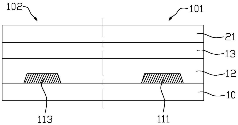
[0032] A substrate 10 is provided. The substrate 10 includes a display area 101 and a non-display area 102 located on the periphery of the display area 101 . The array substrate is fabricated on the substrate 10 at the same time. Specifically, the substrate 10 is a transparent substrate 10, for example made of glass.

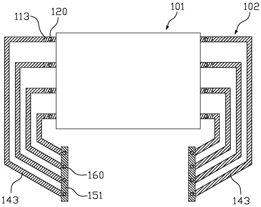
[0033] A first metal layer (not shown) is formed on the substrate 10, and the first metal layer is patterned to form gates 111 and scan lines (not shown) in the display area 101, and form The first lead 113 of the area 102 is electrically connected to the scan line. Specifically, the material of the first metal layer is made of stacked Mo (molybdenum), Al (aluminum), and Mo (molybdenum), and the first metal layer is exposed, developed and etched, thereby forming the gate 111, scanning wire and the first lead 11...

Embodiment 2

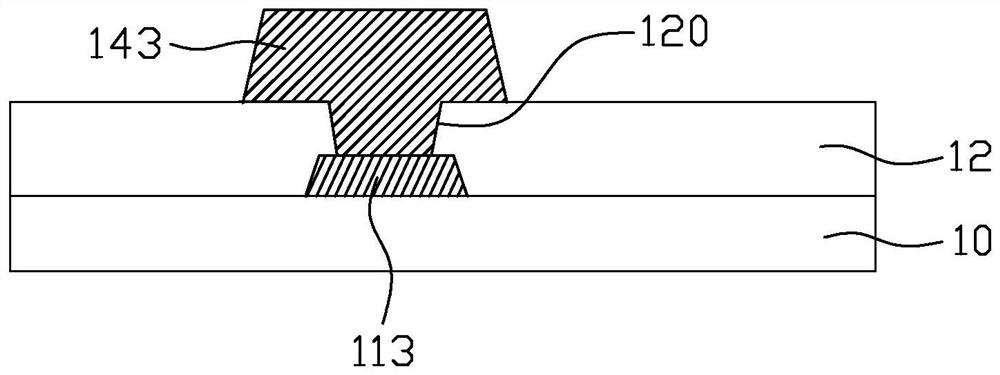
[0058] The part of this embodiment is the same as that of Implementation 1, and the same part will not be repeated here. The difference is that: Figure 5a to Figure 5l As shown, before the step of forming the first contact hole 120 penetrating through the active layer film 13 and the first insulating layer 12, the active layer film 13 is patterned to form silicon islands 131 in the display area 101, and in the non- An etching guide 132 is formed in the display area 102 , and the etching guide 132 corresponds to the position of the first contact hole 120 .

[0059] Specifically, such as Figure 5a to Figure 5c As shown, the fourth photoresist layer 24 is coated on the active layer film 13, and after exposure, development and etching, a part of the active layer film 13 remains at the position where the first contact hole 120 is formed, as a guide for subsequent etching. Or transition, that is, etch the guide portion 132 . Such as Figure 5d As shown, the fourth photoresist l...


PUM


Abstract

The invention provides a manufacturing method of an array substrate and the array substrate. A first insulating layer and an active layer film which cover a first metal layer are sequentially formed on a substrate, the etching rate of the active layer film is higher than that of the first insulating layer, and the active layer film and the first insulating layer are stacked up and down. The activelayer thin film is used as a guide layer of the first insulating layer during trepanning, and the active layer thin film and the first insulating layer are trepanned at the positions corresponding tothe first contact holes, so that the first contact holes penetrating through the active layer thin film and the first insulating layer from top to bottom can be formed. The etching rates of the active layer film and the first insulating layer are different, through the guidance of the active layer film during trepanning, the good taper angles can be obtained at the positions of the first contactholes while the undercut problem of the first insulating layer below is avoided, so that the risk of breakage of the second metal layers subsequently filled into the first contact holes is avoided, the product yield is effectively improved, a new photomask is not needed, and the cost is saved.

Description

technical field [0001] The present invention relates to the field of display technology, in particular to a method for manufacturing an array substrate and the array substrate. Background technique [0002] Liquid crystal display devices have the advantages of good picture quality, small size, light weight, low driving voltage, low power consumption, no radiation, and relatively low manufacturing costs. They dominate the field of flat panel displays and are widely used in LCD TVs, mobile phones, In electronic devices such as personal digital assistants (PDAs), digital cameras, computer screens, or laptop screens. The liquid crystal display device includes an opposite color filter substrate (Color Filter, CF) and a thin film transistor array substrate (TFT array) and a liquid crystal layer (LC layer) sandwiched between them. [0003] In the traditional manufacturing process of thin film transistor array substrates, it is sometimes necessary to open through holes on the insul...

Claims


Application Information

Patent Timeline
Patent Type & Authority Applications(China)
IPC IPC(8): H01L21/84H01L27/12
CPCH01L27/1259H01L27/1244
Inventor 柯健王龙勃王亮李治朝
Owner KUSN INFOVISION OPTOELECTRONICS
Why Eureka
Try Eureka