
Two-dimensional transition metal chalcogenide wave-absorbing material as well as preparation method and application thereof

A transition metal chalcogenide, wave absorbing material technology, applied in vanadium compounds, tungsten compounds, chemical instruments and methods, etc., can solve the problems of limited wave absorption performance, high wave absorption matching thickness, poor impedance matching, etc., and achieve excellent impedance. Matching characteristics and obvious advantages

Active Publication Date: 2020-11-20
NINGBO INST OF MATERIALS TECH & ENG CHINESE ACADEMY OF SCI
View PDF3 Cites 0 Cited by
  • Summary
  • Abstract
  • Description
  • Claims
  • Application Information

AI Technical Summary

Problems solved by technology

[0007] However, most of the TMDs absorbing materials reported at present have the disadvantages of poor impedance matching, high absorbing matching thickness (4mm or even 8mm), and limited absorbing performance, which are difficult to meet the needs of the rapid development of the electromagnetic field.

Method used


Image

  • Two-dimensional transition metal chalcogenide wave-absorbing material as well as preparation method and application thereof
  • Two-dimensional transition metal chalcogenide wave-absorbing material as well as preparation method and application thereof
  • Two-dimensional transition metal chalcogenide wave-absorbing material as well as preparation method and application thereof

Examples


Embodiment 1

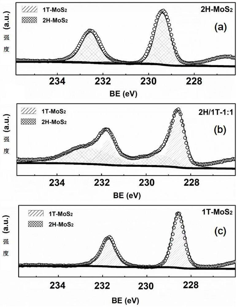
[0040] (1) Weigh the corresponding mass of ammonium thiomolybdate and thiourea according to the molar ratio of 1:5, and place them in a 50mL beaker. Add 20mL of nitrogen methylpyrrolidone and 5mL of ethanol and stir thoroughly for 1h to obtain a mixed solution; transfer the obtained reaction solution to a solvothermal reaction inner liner with a capacity of 50mL, place the inner liner in a stainless steel outer sleeve and seal it, React at 200°C for 15 hours.

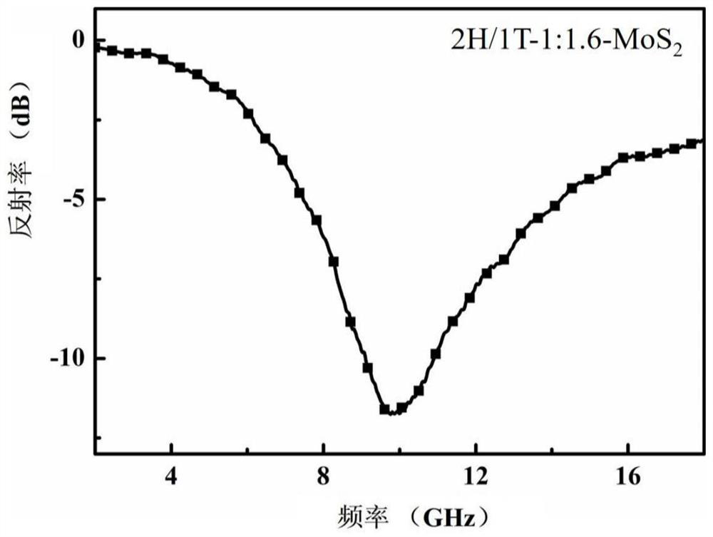
[0041] (2) After the reaction, the product was placed in a centrifuge tube and centrifuged at 10,000 rpm for 20 minutes at high speed, and the product at the bottom of the tube was washed with deionized water and absolute ethanol for 2 to 3 times, and dried in an oven at 50°C for 15 hours to obtain the final product 2H / 1T-1:1.6-MoS 2 Absorbing material.

Embodiment 2

[0043] According to the preparation process of Example 1, the only difference is that the reaction solvent in step (1) is replaced by 27mL nitrogen methyl pyrrolidone and 3mL ethanol to obtain 2H / 1T-1:1-MoS 2 Absorbing material.

Embodiment 3

[0045] According to the preparation process of Example 1, the only difference is that the reaction solvent in step (1) is replaced by 28mL nitrogen methyl pyrrolidone and 2mL ethanol to obtain 2H / 1T-1:0.4-MoS 2 Absorbing material.


PUM

PropertyMeasurementUnit
Sizeaaaaaaaaaa
Reflectivityaaaaaaaaaa
Maximum reflectivityaaaaaaaaaa

Abstract

The invention relates to the field of electromagnetic functional materials, and discloses a two-dimensional transition metal chalcogenide wave-absorbing material as well as a preparation method and application thereof. The preparation method of the wave-absorbing material comprises the following steps: dissolving a transition metal source and a chalcogen source in a solvent, carrying out solvothermal reaction, and finally processing to obtain the two-dimensional transition metal chalcogenide wave-absorbing material; wherein the solvent is a mixed solution of N-methyl pyrrolidone and an alcoholreagent. According to the method, the volume ratio of the N-methyl pyrrolidone to the alcohol reagent in the reaction solvent is regulated and controlled; and the ratio of a semiconductor phase (2H)to a metal phase (1T) in the prepared wave-absorbing material is accurately regulated and controlled, so that the wave-absorbing material with remarkable advantages in indexes such as matching characteristics, maximum reflectivity and effective bandwidth is obtained, and the material can be applied to the fields of high-frequency electromagnetic compatibility and related electromagnetic protection.

Description

technical field [0001] The invention relates to the field of electromagnetic wave absorbing materials, in particular to a two-dimensional transition metal chalcogenide wave absorbing material, its preparation method and application. Background technique [0002] At present, with the rapid development of information technology, electromagnetic absorbing materials play an increasingly important role in military stealth, electronic communication and other fields. As a new two-dimensional material, two-dimensional transition metal dichalcogenides (TMDs) have good physical and chemical properties, thermal stability and mechanical flexibility, and their related research in the field of dielectric wave absorption has gradually attracted attention. [0003] in MoS 2 As a representative, the applicant prepared and reported two-dimensional molybdenum disulfide (MoS2) for the first time in 2015 2 ) Dielectric absorbing properties of nanosheets. The experimental results show that: Mo...

Claims


Application Information

Patent Timeline
IPC IPC(8): C01G39/06C01G31/00C01G41/00H05K9/00
CPCC01G39/06C01G31/00C01G41/00H05K9/0081C01P2002/85C01P2004/04
Inventor 宁明强满其奎谭果果李润伟
Owner NINGBO INST OF MATERIALS TECH & ENG CHINESE ACADEMY OF SCI
Learn More