Magnetic field detector based on metal-medium-metal waveguide
A detector and light detector technology, applied in the field of magnetic field detection, can solve the problem of low sensitivity of magnetic field detection and achieve the effect of high sensitivity
- Summary
- Abstract
- Description
- Claims
- Application Information
AI Technical Summary
Problems solved by technology
Method used
Image
Examples
Embodiment 1
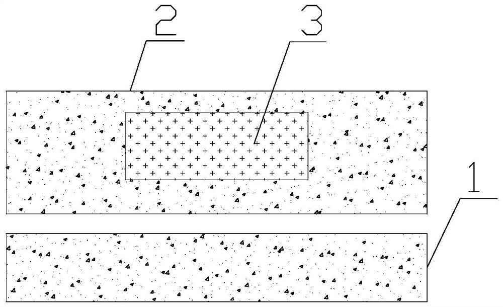
[0021] The invention provides a magnetic field detector based on metal-dielectric-metal waveguide. like figure 1 As shown, the magnetic field detector based on metal-dielectric-metal waveguide includes a light source, a photodetector, a substrate, and a first metal part 1 and a second metal part 2 placed on the substrate. The first metal part 1 and the second metal part 2 are noble metal thin films. The material of the noble metal thin film is gold or silver. The first metal part 1 and the second metal part 2 respectively have mutually parallel interfaces, and the first metal part 1 and the second metal part 2 constitute a metal-dielectric-metal waveguide. The thicknesses of the first metal part 1 and the second metal part 2 are equal. The thickness of the noble metal film is greater than 500 nanometers to confine the electromagnetic wave within the metal-dielectric-metal waveguide. The second metal part 2 is provided with a cavity 3, the cavity 3 is rectangular, and the s...
Embodiment 2
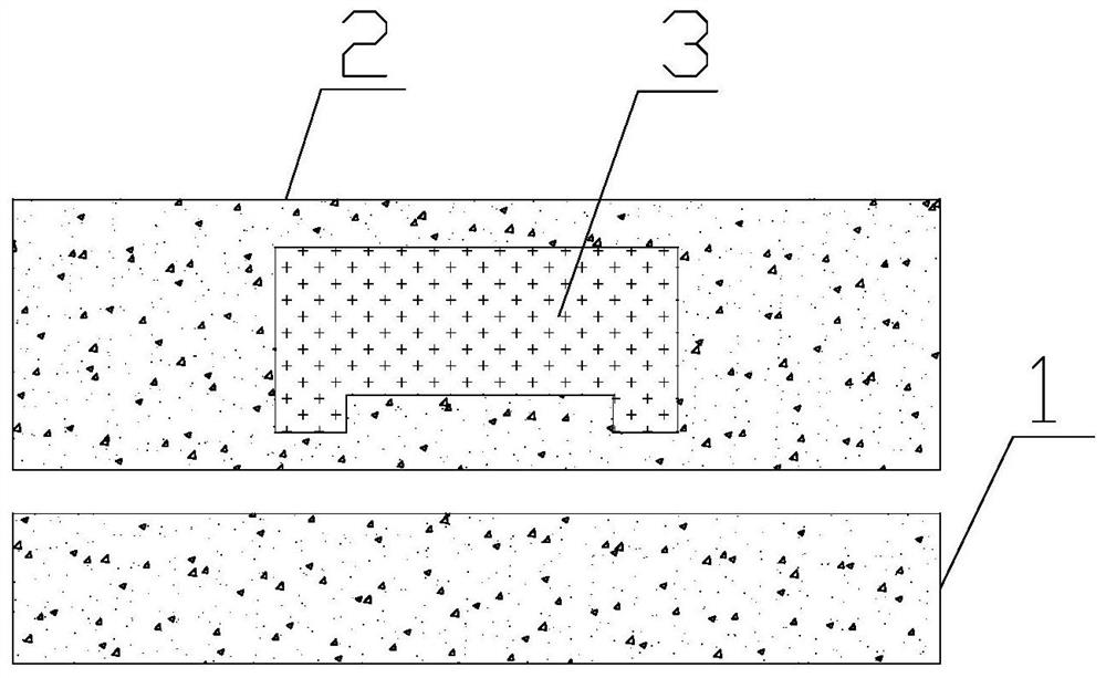
[0026] On the basis of Example 1, such as figure 2 As shown, the cavity 3 also includes two protruding parts, the two protruding parts are respectively arranged at the two ends of the cavity 3 near the metal-dielectric-metal waveguide, and the two protruding parts are also provided with magnetostrictive material. That is to say, along the metal-dielectric-metal waveguide direction, on the side close to the metal-dielectric-metal waveguide, both ends of the cavity 3 have protrusions. There are many magnetostrictive materials at both ends of the cavity 3, and the two ends of the cavity 3 are close to the metal-dielectric-metal waveguide. In this way, when the magnetostrictive material is stretched under the action of the magnetic field, the magnetostrictive material at both ends stretches more, changing the width of the metal-dielectric-metal waveguide more, forming a structural singularity, and the metal- The electromagnetic wave in the dielectric-metal waveguide resonates be...
Embodiment 3
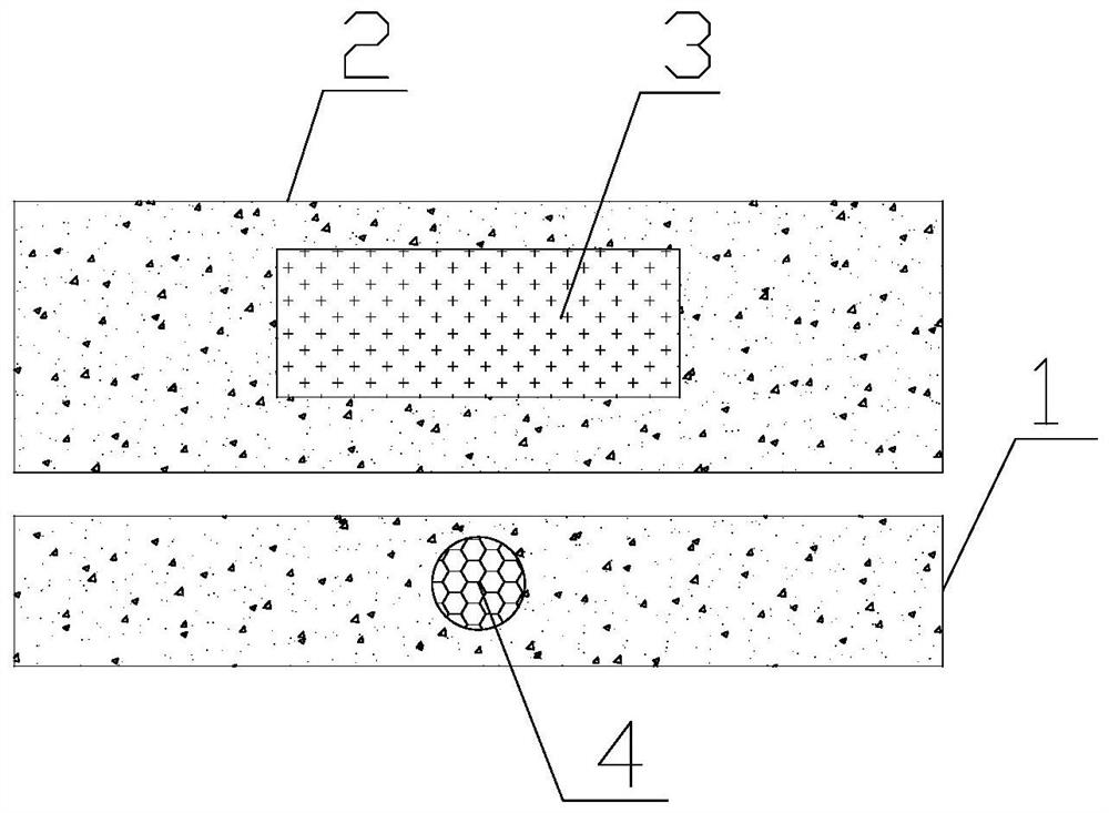
[0029] On the basis of embodiment 1 or 2, such as figure 2 As shown, the first metal part 1 is provided with a second cavity 4, and the second cavity 4 is provided with a magnetostrictive material. The magnetostrictive material in the second cavity 4 may be the same as or different from the magnetostrictive material in the cavity 3 . However, the magnetostrictive material in the second cavity 4 also elongates under the action of the magnetic field. The second cavity 4 is placed in the center of the cavity. In this way, under the action of the magnetic field to be measured, the magnetostrictive material in the second cavity 4 elongates, changing the width of the waveguide corresponding to the center of the cavity 3 from another direction, and changing the transmission of the waveguide more. coefficient, which improves the detection sensitivity.
[0030] Furthermore, the distance between the second cavity 4 and the metal-dielectric-metal waveguide is greater than 100 nanomet...
PUM
| Property | Measurement | Unit |
|---|---|---|
| thickness | aaaaa | aaaaa |
| width | aaaaa | aaaaa |
Abstract
Description
Claims
Application Information


