
Pixel-level ADC focal plane reading circuit and correction method thereof

A technology for reading out circuits and focal planes, which is used in television, electrical components, and image communications. Effect

Pending Publication Date: 2020-11-24
NO 24 RES INST OF CETC
View PDF8 Cites 0 Cited by
  • Summary
  • Abstract
  • Description
  • Claims
  • Application Information

AI Technical Summary

Problems solved by technology

A typical two-point NUC calibration requires zero addition and subtraction and gain multiplication for each pixel. With the expansion of the image area and the increase of the frame rate, the amount of NUC calculations increases sharply, resulting in increased system power consumption and decreased performance.

Method used


Image

  • Pixel-level ADC focal plane reading circuit and correction method thereof
  • Pixel-level ADC focal plane reading circuit and correction method thereof
  • Pixel-level ADC focal plane reading circuit and correction method thereof

Examples


Embodiment Construction

[0022] The following will clearly and completely describe the technical solutions in the embodiments of the present invention with reference to the accompanying drawings in the embodiments of the present invention. Obviously, the described embodiments are only some, not all, embodiments of the present invention. Based on the embodiments of the present invention, all other embodiments obtained by persons of ordinary skill in the art without making creative efforts belong to the protection scope of the present invention.

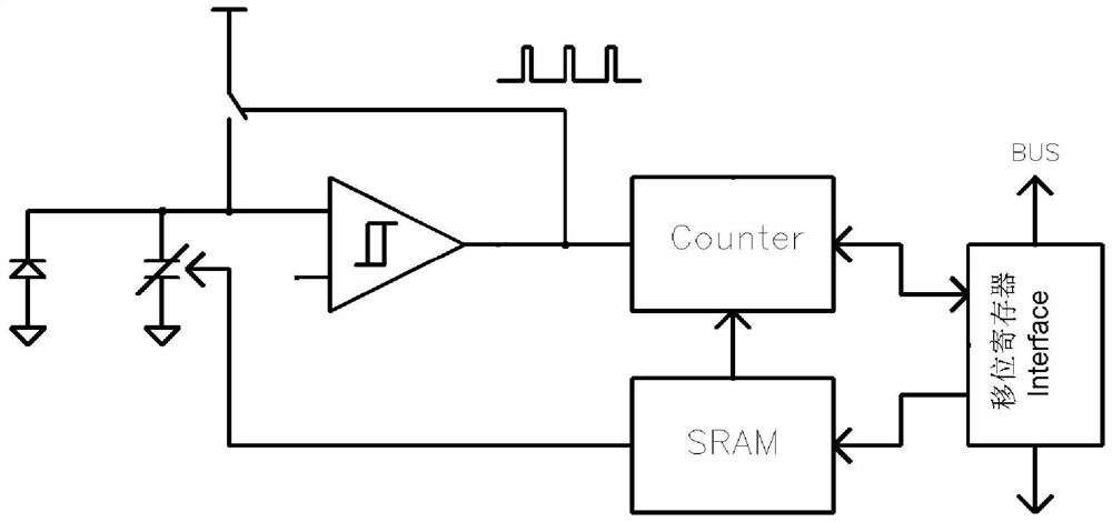
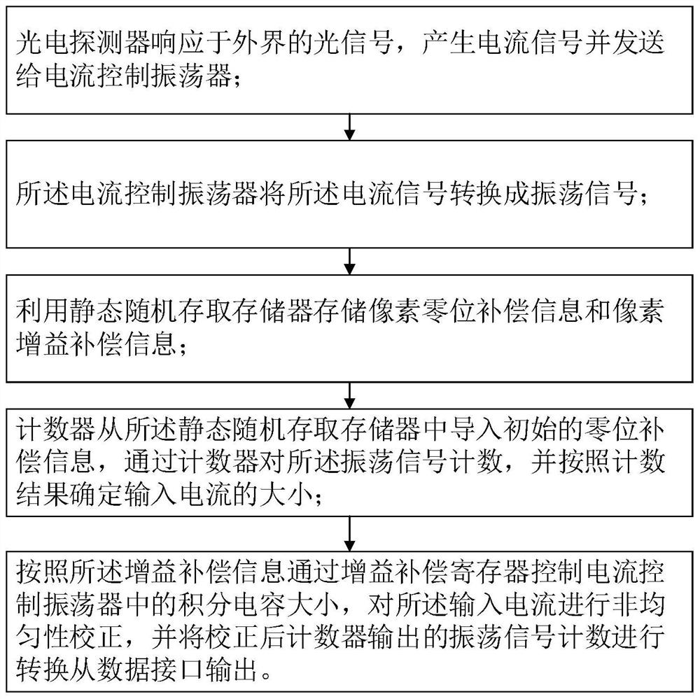
[0023] figure 1 It is a block diagram of the principle architecture of the pixel-level ADC adopted in the present invention, such as figure 1 As shown, in the pixel-level ADC focal plane readout circuit adopted in the present invention, the current generated by the photodetector based on the photoelectric response is converted into a frequency and current intensity by a current-frequency converter (ie, a current-controlled oscillator ICO). The relevant oscill...


PUM


Abstract

The invention is used for focal plane reading circuit design, and particularly relates to a pixel-level ADC focal plane reading circuit and a correction method thereof. The reading circuit comprises aphotoelectric detector, a current control oscillator, a counter, a static random access memory, a shift register and a data bus, wherein the output end of the photoelectric detector is connected withthe input end of the current control oscillator; the output end of the current control oscillator is connected with the input end of the counter; the other input end of the counter is connected withthe output end of the static random access memory, and the output end of the counter is connected to the input end of the shift register; the other output end of the static random access memory is connected with the feedback input end of the current control oscillator; the input end of the static random access memory is connected with the other output end of the shift register; the shift registeris connected with a data bus and outputs a converted current signal; the implementation mode is simple, extra operation resources are not needed, and system power consumption is not increased; and real-time processing is facilitated.

Description

technical field [0001] The invention is used for the design of the focal plane readout circuit, and specifically provides a method for correcting the non-uniformity of the pixel for the readout circuit. Background technique [0002] Due to the influence of material and process non-uniformity, there is inevitably non-uniformity in the response of the focal plane pixel to the optical signal, that is, the same luminous flux input corresponds to different digital outputs, resulting in spatial noise in the final image, which affects The imaging quality of the image; therefore, it is of great significance to perform nonuniformity correction (NUC for short) on the focal plane image. [0003] In the traditional focal plane readout circuit (Readout integrated circuit, referred to as ROIC) technology, the photocurrent signal generated by the detector is accumulated and converted into a voltage signal in the capacitor (electronic well), and then the voltage signal is converted by ADC t...

Claims


Application Information

Patent Timeline
IPC IPC(8): H04N5/378H04N5/217
CPCH04N23/81H04N25/75
Inventor 黄文刚曾岩高炜琪
Owner NO 24 RES INST OF CETC
Learn More