Nonvolatile programmable integrated photonic device and design method thereof

An integrated photon and non-volatile technology, applied in optical components, nonlinear optics, instruments, etc., can solve the problems of unfavorable device smart interconnection, single reconfigurable function, and high energy consumption of devices, so as to improve design freedom and reduce Transmission loss, effect of improving device performance

Active Publication Date: 2020-11-27
HUAZHONG UNIV OF SCI & TECH
View PDF8 Cites 9 Cited by
  • Summary
  • Abstract
  • Description
  • Claims
  • Application Information

AI Technical Summary

Problems solved by technology

In addition, the electro-optic effect and thermo-optic effect are volatile, and require additional energy injection to maintain the existing state even when they are not tuned, so devices based on these two effects have high energy consumption
Existing tunable photonic devices usually only have a few design parameters, and the reconfigurable functions are relatively single, which is not conducive to the realization of intelligent interconnection between devices

Method used


Image

  • Nonvolatile programmable integrated photonic device and design method thereof
  • Nonvolatile programmable integrated photonic device and design method thereof
  • Nonvolatile programmable integrated photonic device and design method thereof

Examples


Embodiment Construction

[0028] In order to make the object, technical solution and advantages of the present invention clearer, the present invention will be further described in detail below in conjunction with the accompanying drawings and embodiments. It should be understood that the specific embodiments described here are only used to explain the present invention, not to limit the present invention. In addition, the technical features involved in the various embodiments of the present invention described below can be combined with each other as long as they do not constitute a conflict with each other.

[0029] In the present invention, the terms "first", "second" and the like (if any) in the present invention and drawings are used to distinguish similar objects, and are not necessarily used to describe a specific order or sequence.

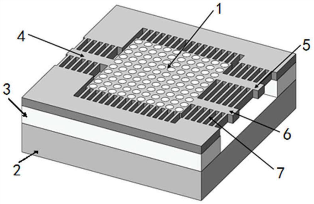
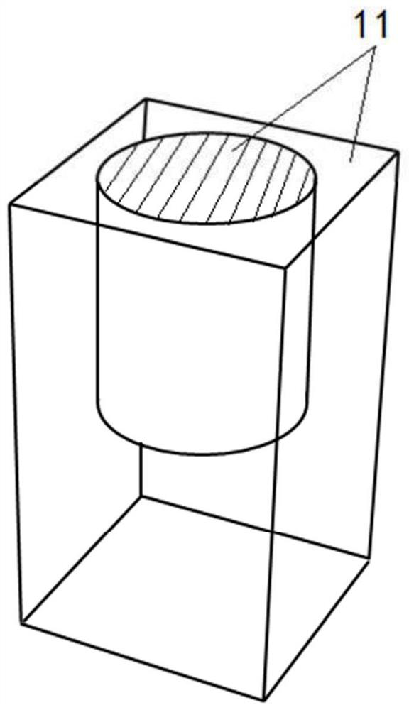
[0030] figure 1 Schematic diagram of the structure of the non-volatile programmable integrated photonic device proposed by the present invention. refer to figur...


PUM

PropertyMeasurementUnit
heightaaaaaaaaaa
diameteraaaaaaaaaa
depthaaaaaaaaaa

Abstract

The invention discloses a nonvolatile programmable integrated photonic device and a design method thereof, and belongs to the field of photonic devices. A multimode waveguide of the integrated photonic device comprises N*M logic units capable of independently adjusting tuning states, and N and M are positive integers; each logic unit comprises a cuboid structure which is provided with a groove andmade of silicon and a filling structure which is filled in the groove and made of a phase change material, and each logic unit is of a sub-wavelength size structure. By adjusting the tuning state ofeach logic unit, the distribution of the refractive indexes of the device is adjusted and controlled in the sub-wavelength scale, and photonic devices with different functions are realized. The phasechange material is combined with a photonic-like crystal structure; the non-volatile and programmable ultra-small integrated photonic device is realized by utilizing the non-volatile and reconfigurable characteristics of the phase change material and utilizing the light field regulation and control capability of the sub-wavelength scale of the photonic-like crystal structure, the device size and energy consumption are reduced, and more tuning functions are realized, so that different functional purposes are realized.

Description

technical field [0001] The invention belongs to the field of photonic devices, and more specifically relates to a nonvolatile programmable integrated photonic device and a design method thereof. Background technique [0002] With the development of high-performance computing and high-speed interconnection, copper wires are gradually unable to meet the needs of high-speed data transmission. All-optical interconnection has the advantages of large bandwidth and long-distance transmission, and is considered as a promising solution. To realize low-cost all-optical interconnects, integrated photonic devices have become a hot research area in both academia and industry. Silicon-based integrated photonic devices are highly integrated and compatible with the CMOS platform, and are one of the most popular research directions in the field of optoelectronics. How to integrate more devices in a limited area, realize the intelligent interconnection between devices, and reduce chip energ...

Claims


Application Information

Patent Timeline
Patent Type & Authority Applications(China)
IPC IPC(8): G02B6/12G02B27/00G02F1/01
CPCG02B6/12004G02B6/12007G02B27/0012G02F1/011G02F1/0147
Inventor 张敏明杨思康刘德明
Owner HUAZHONG UNIV OF SCI & TECH
Why Eureka
Try Eureka