Packaging structure for integrated circuit design

A technology of integrated circuits and packaging structures, which is applied in the direction of circuits, electrical components, and electrical solid devices, and can solve problems such as poor practicability, inability to adapt to different sizes of integrated circuit boards, and inability to conveniently realize docking and fixing, etc., to achieve strong applicability, Guaranteed stable effect

Active Publication Date: 2020-11-27
深圳市杰驰电子有限公司
View PDF16 Cites 2 Cited by
  • Summary
  • Abstract
  • Description
  • Claims
  • Application Information

AI Technical Summary

Problems solved by technology

[0003] In the installation process of integrated circuits, in order to ensure the stability of its installation, it is necessary to design and consider the packaging structure for integrated circuits. The existing packaging structure cannot adapt to integrated circuit boards of different sizes, and it cannot be conveniently connected and fixed during installation and docking. Poor practicality

Method used


Image

  • Packaging structure for integrated circuit design
  • Packaging structure for integrated circuit design
  • Packaging structure for integrated circuit design

Examples


Embodiment Construction

[0020] The following will clearly and completely describe the technical solutions in the embodiments of the present invention with reference to the accompanying drawings in the embodiments of the present invention. Obviously, the described embodiments are only some, not all, embodiments of the present invention. Based on the embodiments of the present invention, all other embodiments obtained by persons of ordinary skill in the art without making creative efforts belong to the protection scope of the present invention.

[0021] Unless otherwise defined separately, directions such as up, down, left, right, front, back, inside and outside referred to herein are up, down, left, right, front and back in the drawings shown in the present invention. , inside and outside directions shall prevail, which shall be explained together here.

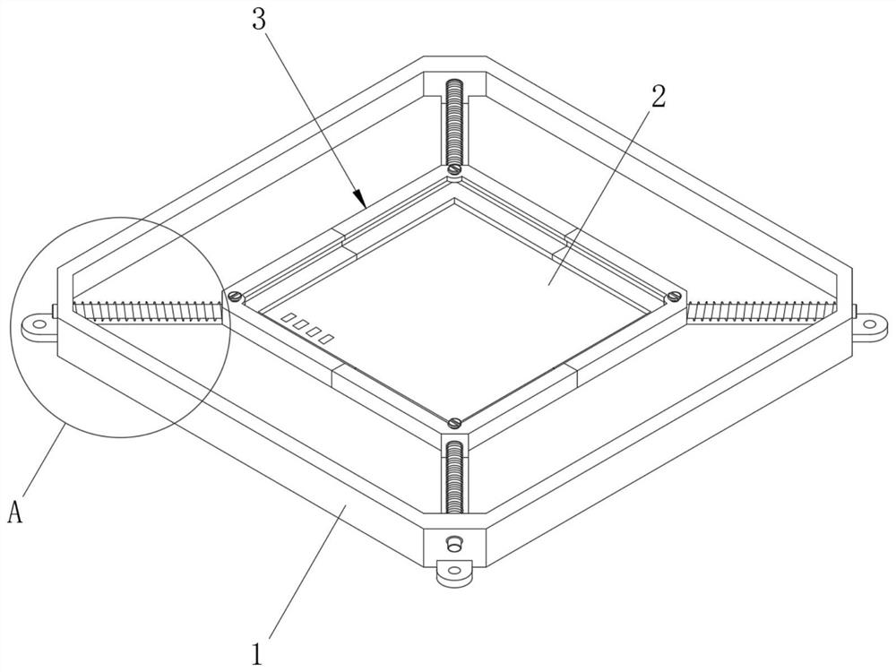
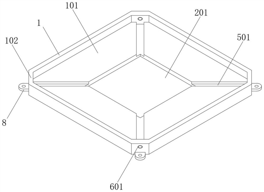
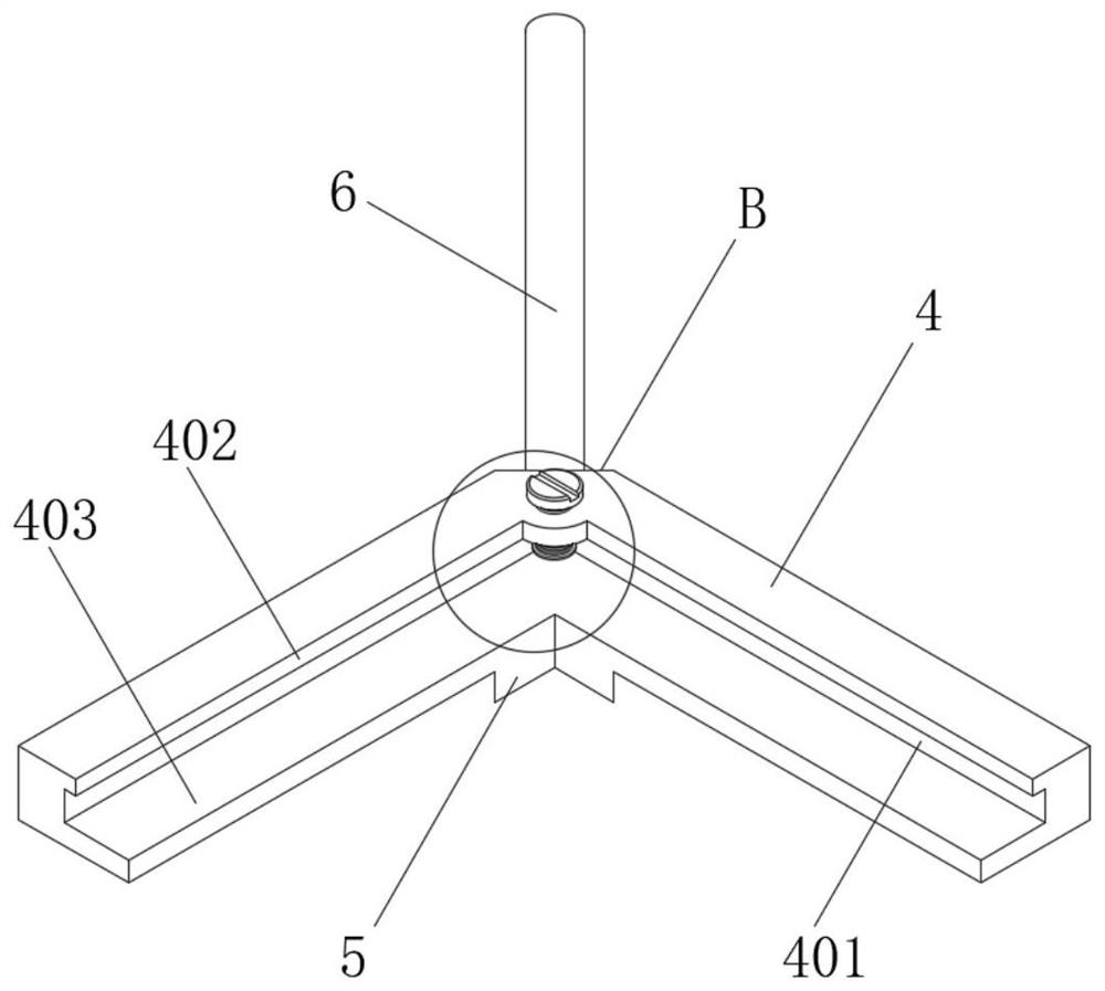
[0022] The present invention provides such Figure 1-5 A packaging structure for integrated circuit design is shown, including a docking substrate ...


PUM


Abstract

The invention discloses a packaging structure for integrated circuit design. The packaging structure comprises a butt joint substrate, an integrated circuit butt joint plate and a clamping mechanism.The butt joint substrate is of a rectangular plate-shaped structure. A clamping groove is formed in the upper end face of the butt joint base plate. The center of the clamping groove of the butt-jointsubstrate is provided with a butt-joint plate installation groove matched with an integrated circuit butt-joint plate. The butt-joint substrate is clamped and limited at the periphery of the integrated circuit butt-joint plate through the butt-joint plate mounting groove; the integrated circuit butt-joint plate is of a rectangular plate-shaped structure, pins in butt joint with an integrated circuit are constructed on the upper end face of the integrated circuit butt-joint plate, and substrate chamfers are constructed at the four corners of the butt-joint substrate; clamping mechanisms are arranged on the sides, facing the integrated circuit butt-joint plate, of the four sets of substrate chamfers in a matched mode. The packaging structure for the integrated circuit design is reasonable in structure, the integrated circuit can be packaged and fixed easily and conveniently, and the packaging structure is high in applicability and high in practical value.

Description

technical field [0001] The invention belongs to the technical field of integrated circuits, and in particular relates to a packaging structure for integrated circuit design. Background technique [0002] An integrated circuit is a tiny electronic device or component. Using a certain process, the transistors, resistors, capacitors, inductors and other components required in a circuit are interconnected, and they are fabricated on a small or several small semiconductor wafers or dielectric substrates, and then packaged in a tube. , and become a microstructure with required circuit functions; all the components in it have been structurally integrated, making electronic components a big step towards miniaturization, low power consumption, intelligence and high reliability. It is represented by the letter "IC" in the circuit. The inventors of the integrated circuit are Jack Kilby (germanium (Ge)-based integrated circuits) and Robert Noyce (silicon (Si)-based integrated circuits...

Claims


Application Information

Patent Timeline
Patent Type & Authority Applications(China)
IPC IPC(8): H01L23/32
CPCH01L23/32
Inventor 陈瑜珍
Owner 深圳市杰驰电子有限公司
Why Eureka
Try Eureka