Array substrate and display panel
An array substrate and pad technology, which is applied in the field of array substrates and display panels, can solve the problems of abnormal display and short circuit of conductive particles of conductive adhesive, and achieve the effects of avoiding short circuit, increasing height difference and improving product yield.
- Summary
- Abstract
- Description
- Claims
- Application Information
AI Technical Summary
Problems solved by technology
Method used
Image


Examples
Embodiment 1
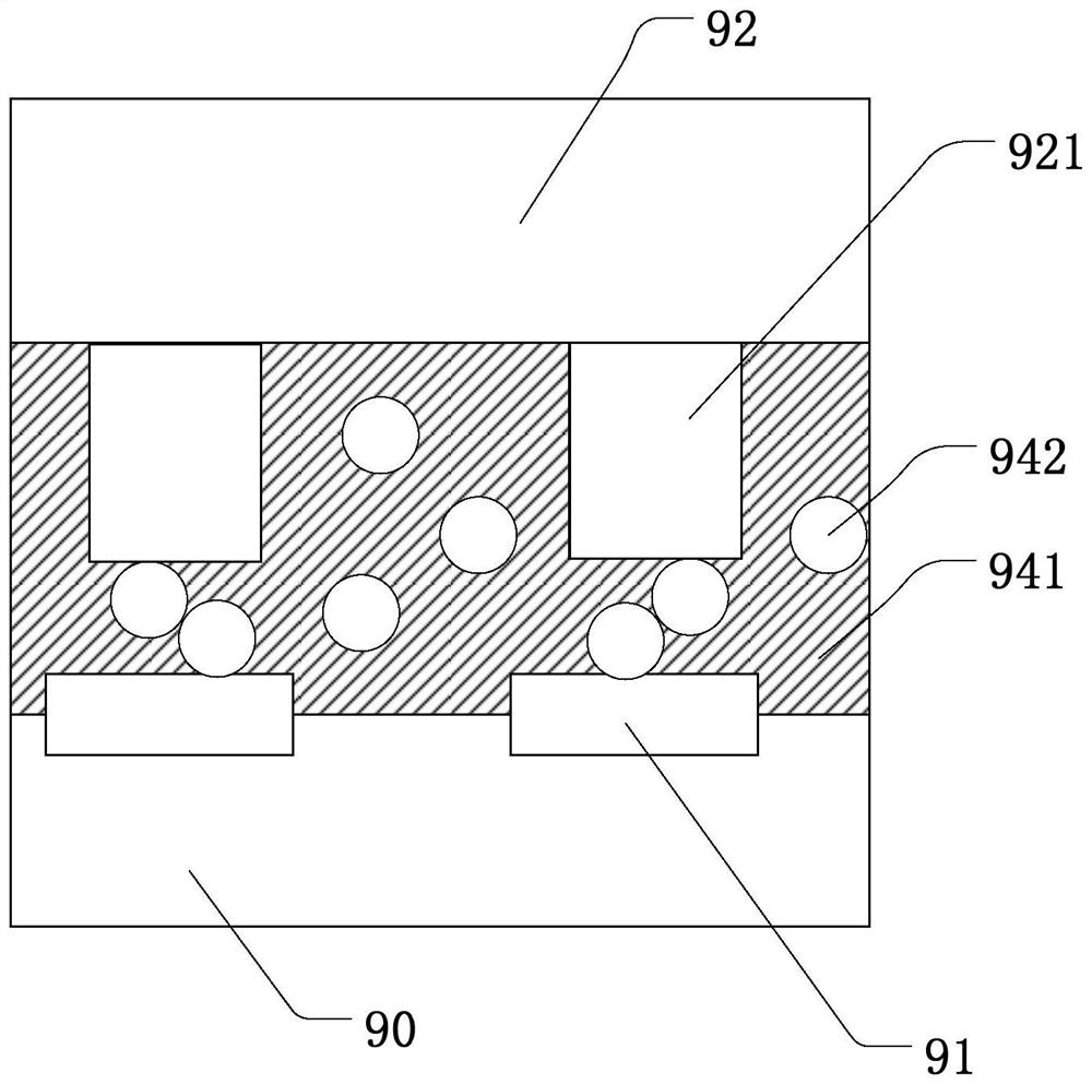
[0037] see Figure 7 , Figure 8 As shown, in Embodiment 1 of the present invention, an array substrate 100 is provided, which is provided with a binding area, and the binding area includes a substrate layer 1, a first metal layer 2, and an interlayer insulating layer stacked in sequence from bottom to top. 3. The second metal layer 4 , the passivation layer 5 and the conductive layer 6 .
[0038]Specifically, the first metal layer 2 is disposed on the substrate layer 1, and is provided with a plurality of pad bottoms 21 arranged at intervals; the interlayer insulating layer 3 is disposed on the first metal layer 2 , a plurality of grooves 31 and a plurality of via holes 32 are provided; the grooves 31 are correspondingly provided between two adjacent pad bottoms 21; the via holes 32 are provided correspondingly to the pad bottoms 21; the The second metal layer 4 is disposed on the interlayer insulating layer 3, and is provided with a plurality of spaced wires 41 and a line ...
Embodiment 2
[0049] see Figure 9 , Figure 10 As shown, in embodiment 2, most of the technical features in embodiment 1 are included. The difference is that in embodiment 2, a plurality of grooves 31 are provided between two adjacent pad bottoms 21, each One spacing wire 41 is disposed in the groove 31 . In Embodiment 1, one groove 31 is not provided between two adjacent pad bottoms 21 .
[0050] In this embodiment, two spaced traces 41 are set between two adjacent pad bottoms 21, and two grooves 31 are correspondingly set between two adjacent pad bottoms 21. The distance between the two grooves 31 is 3.5um-4.5um, preferably 4um.
Embodiment 3
[0052] In Embodiment 3, accommodating grooves (not shown) may be further provided on the substrate layer 1 corresponding to the positions of the grooves 31, so as to further increase the height of the spaced traces 41 and the pads used for bonding. Poor, avoiding the conductive particles in the bonding conductive adhesive being pressed on the spacer wiring 41 when the bonding is misplaced, and causing a short circuit in the interconnection, which improves the product yield.
[0053] The present invention also provides a display panel, including the above-mentioned array substrate 100 .
[0054] Compared with the prior art, the beneficial effect of the display panel provided by the embodiment of the present invention is the same as the beneficial effect of the array substrate 100 provided by the above technical solution, which will not be repeated here.
[0055] Wherein, the display panel provided in the above embodiments may be any product or component with a display function,...
PUM
| Property | Measurement | Unit |
|---|---|---|
| Width | aaaaa | aaaaa |
| Thickness | aaaaa | aaaaa |
| Thickness | aaaaa | aaaaa |
Abstract
Description
Claims
Application Information
 - R&D
- Intellectual Property
- Life Sciences
- Materials
- Tech Scout
- Unparalleled Data Quality
- Higher Quality Content
- 60% Fewer Hallucinations
Browse by: Latest US Patents, China's latest patents, Technical Efficacy Thesaurus, Application Domain, Technology Topic, Popular Technical Reports.
© 2025 PatSnap. All rights reserved.Legal|Privacy policy|Modern Slavery Act Transparency Statement|Sitemap|About US| Contact US: help@patsnap.com