A method for forming chip metal bumps

A technology of metal bumps and molding methods, which is applied in the direction of semiconductor devices, electrical components, circuits, etc., to overcome the limitation of photoresist ability, reduce costs, and improve the effect of ball forming quality

Active Publication Date: 2022-04-08
CHIPMORE TECH CORP LTD +1
View PDF0 Cites 0 Cited by
  • Summary
  • Abstract
  • Description
  • Claims
  • Application Information

AI Technical Summary

Problems solved by technology

[0005] The purpose of the present invention is to provide a method for forming chip metal bumps to solve the deficiencies in the prior art. It can overcome the limitation of photoresist ability through the existing electroplating process conditions, increase the amount of electroplating tin, and make implants Large-size solder ball bumps that can only be formed with small balls, resulting in improved ball forming quality and more flexible process applications

Method used


Image

  • A method for forming chip metal bumps
  • A method for forming chip metal bumps
  • A method for forming chip metal bumps

Examples


Embodiment 1

[0049] In this embodiment, the first electroplating layer 50 is electroplated after all the photoresist layers are formed, and after the panes are formed on all the photoresist layers, electroplating is performed in the lowermost pane. In the first electroplating layer 50 After the electroplating is formed, the metal bump 60 is formed by electroplating on the upper surface of the first electroplating layer 50 , that is, the first electroplating layer 50 and the metal bump 60 are sequentially electroplated and formed.

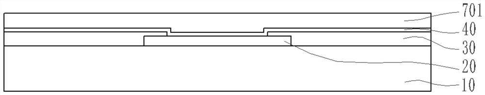
[0050] Specifically, such as Figure 3-9 As shown, there are three photoresist layers formed in this embodiment, namely the first photoresist layer 701, the second photoresist layer 702 and the third photoresist layer 703; correspondingly, the first photoresist layer 701, the second photoresist layer Corresponding first panes 801 , second panes 802 and third panes 803 are respectively formed on the resist layer 702 and the third photoresist layer 703 . The firs...

Embodiment 2

[0053] In this embodiment, the first electroplating layer 50 is formed by electroplating before all the photoresist layers are formed, and the metal bump 60 is formed by electroplating after all the photoresist layers are formed.

[0054] The first electroplating layer 50 is formed by electroplating in the lowermost pane before forming the last photoresist layer; the metal bump 60 is formed on the first electroplating layer 50 after all the photoresist layers are formed.

[0055] The first electroplating layer 50 can be electroplated and formed in the lowermost pane after the lowermost photoresist layer forms the pane, and formed on the upper surface and the lowermost side of the first electroplating layer 50 after forming the first electroplating layer 50. A photoresist layer is formed on the upper surface of the lower photoresist layer, and the panes formed on the photoresist layer cover the first electroplating layer 50 . Then continue to form multi-layer photoresist layers...

Embodiment 3

[0059] In the above-mentioned embodiments, the metal bumps 60 are formed directly on the first electroplating layer 50. Although they can continue to grow on other positions in the pane, due to the part of the photoresist layer exposed outward through the pane The seed layer is not covered so the shape of the metal bumps 60 formed at these locations is not good. In this embodiment, in order to better realize the growth of the metal bump 60, before the last photoresist layer is formed and after the first plating layer 50 is formed on the lowermost pane, the penultimate layer of photoresist The upper surface of the layer, the upper surface of the first electroplating layer 50 and the upper surface of the part of the photoresist layer exposed outward through the window pane cover the second seed layer 90; the metal bump 60 is formed after the last layer of photoresist layer forms the window pane Electroplating is formed on the upper surface of the second seed layer 90 . In this ...


PUM

PropertyMeasurementUnit
thicknessaaaaaaaaaa

Abstract

The invention discloses a method for forming a chip metal bump, which comprises the following steps: providing a silicon substrate, a pad and a passivation layer are formed on the upper surface of the silicon substrate; The surface is covered with the first seed layer; several layers of photoresist layers are sequentially formed on the upper surface of the first seed layer, and part of the photoresist layer is removed on each layer of photoresist layer to form a pane; wherein, the upper and lower adjacent Among the two panes of , the size of the upper pane is larger than the size of the lower pane and the upper pane covers the lower pane; the first seed in the lowermost pane A first electroplating layer is formed on the upper surface of the first electroplating layer, a metal bump is formed on the first electroplating layer, and finally a reflow process is used to form the metal bump into a metal ball. The present invention overcomes the limitation of photoresist ability through the existing electroplating process conditions, increases the amount of electroplated tin and electroplates into balls, improves the quality of balls and reduces the cost.

Description

technical field [0001] The invention relates to the technical field of chip packaging, in particular to a method for forming chip metal bumps. Background technique [0002] Representative examples of packaging technologies include Ball Grid Array (BGA), Flip Chip, Chip Scale Package (CSP) based on area array and surface-mount packages. . [0003] Among the packaging technologies described above, chip-scale packaging is a packaging technology that can make a package as small as a developed real chip. In particular, in Wafer-Level Chip Scale Package (WLCSP), packaging is performed at the wafer level so that the cost per chip can be significantly reduced. WLCSP is a packaging technology that performs packaging and testing on the entire wafer and then cuts it to obtain a single finished chip. The size of the packaged chip is the same as that of the bare chip. Wafer-level packaging complies with the requirements of high integration and miniaturization of semiconductor devices....

Claims


Application Information

Patent Timeline
Patent Type & Authority Patents(China)
IPC IPC(8): H01L21/60
CPCH01L24/03H01L24/11H01L2224/03462H01L2224/11462H01L2224/11
Inventor 黄文杰
Owner CHIPMORE TECH CORP LTD
Why Eureka
Try Eureka