

Transfer device
A technology for transferring equipment and bonding glue, which is applied in the manufacture of conveyor objects, electrical components, semiconductor/solid-state devices, etc., and can solve the problem that LEDs cannot be transferred to display backplanes, etc.
- Summary
- Abstract
- Description
- Claims
- Application Information
AI Technical Summary
Problems solved by technology
Method used
Image

Examples
Embodiment Construction
[0032] The specific embodiments of the present invention will be described in detail below in conjunction with the accompanying drawings. It should be understood that the specific embodiments described here are only used to illustrate and explain the present invention, and the present invention is not limited to the following specific embodiments.
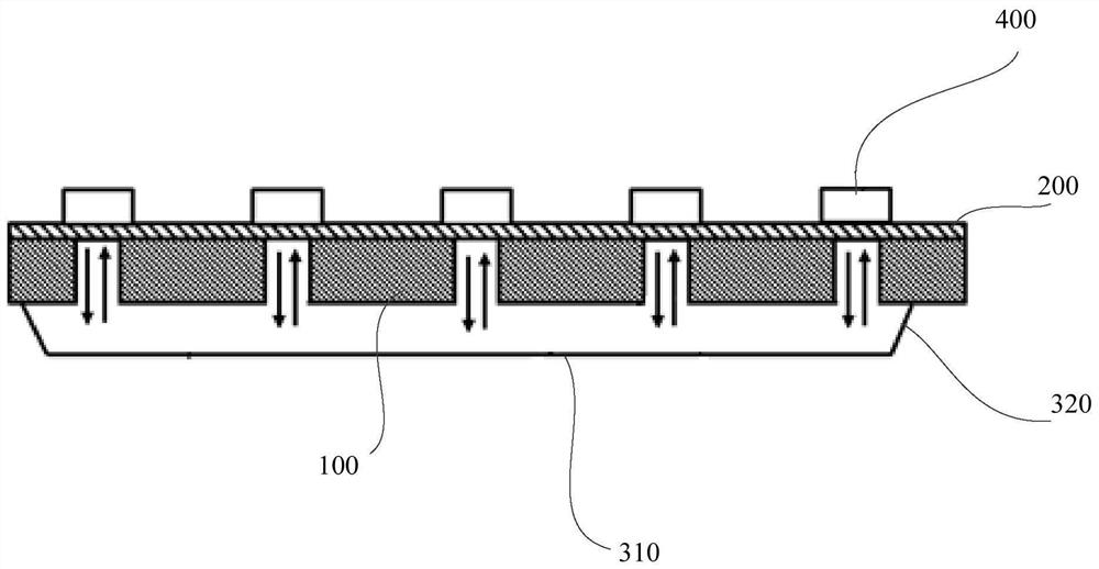
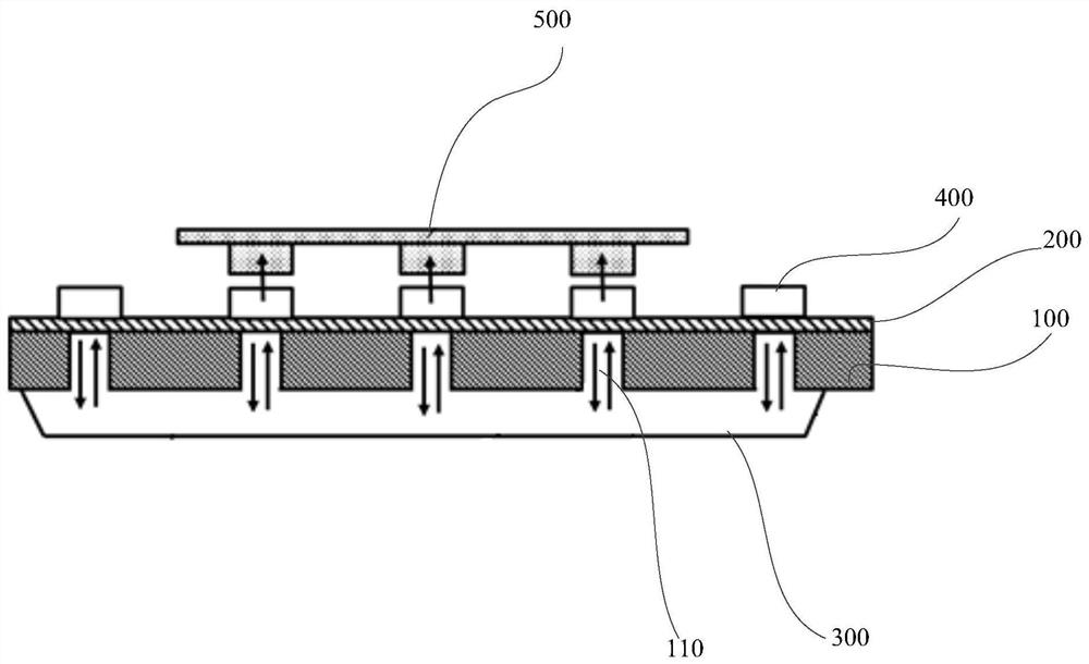
[0033] At present, in the transfer process of LED chips, in order to facilitate the receiving of LED chips, the surface of the temporary substrate is usually provided with an adhesive layer with high adhesion. However, when transferring the LED chips from the temporary substrate to the display backplane, too high Adhesive force will cause some LED chips to be adhered to the adhesive layer, resulting in transfer failure.
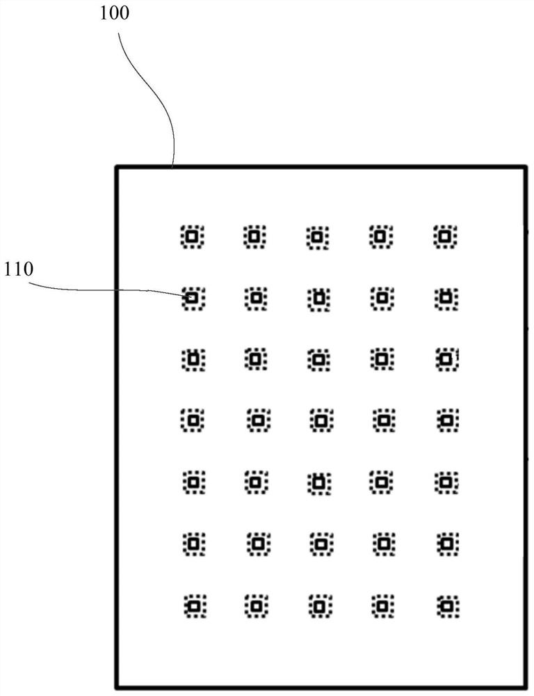
[0034] figure 1 It is a structural schematic diagram of the transfer device of the present invention; figure 2 for figure 1 Schematic diagram of the structure of the temporary substrate; image 3 It is a schem...
PUM
 Abstract
Description
Claims
Application Information