
IO expansion chip

An expansion chip and chip technology, applied in the field of IO expansion chips, can solve the problems of increasing system hardware circuit complexity, hardware circuit complexity, unfavorable pin utilization, etc., to achieve reliable and more accurate collection, precise protection logic control function, The effect of simple wiring

Pending Publication Date: 2020-12-08
广东省大金创新电子有限公司
View PDF0 Cites 5 Cited by
  • Summary
  • Abstract
  • Description
  • Claims
  • Application Information

AI Technical Summary

Problems solved by technology

However, in the specific implementation method, sampling the peripheral IO interface that comes with the CPU, or using a general IO expansion chip to realize the real-time logic of this type of protection, it is difficult to meet the real-time requirements for program operation and processing relying on the CPU, so generally The practice is to use an additional peripheral control circuit to realize the hardware logic protection that detects the blockade. For this reason, the hardware circuit becomes complicated, and the consistency of its control and the flexibility of parameter adjustment are also limited by hardware characteristics and hardware parameters. , and reduces the reliability
Moreover, the general IO expansion chip has low driving capability, and the continuous current is generally less than 10mA
Driving common loads such as relays requires external expansion of driver chips or circuits, which will continue to increase the complexity of system hardware circuits
[0006] In addition, the general IO expansion chip has a fixed pin configuration, the number of input and output ratios and pin positions, which is not conducive to improving the utilization of the pins and is not convenient for wiring.

Method used


Image

  • IO expansion chip
  • IO expansion chip

Examples


specific Embodiment 1

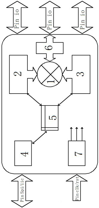
[0033] like figure 1 As shown, the IO configuration module 1 is used to select and control the connection of the IO input acquisition filter module 2, the IO output control module 3 and the specific pins outside the chip; the configuration data is transmitted from the external MCU through the MCU communication interface module 4 and the internal bus control module 5 write;

[0034] IO input acquisition filter module 2, the configuration selection is connected to the external Pin pin of the chip, the high and low level status of the pin is collected, and then the high and low level counts are performed. When the high level count is greater than the value of N1, the signal "1" is recorded, and the low level counts When it is greater than the value of N2, the signal "0" is recorded, and the signal remains unchanged in other states; the values ​​of N1 and N2 are written by the internal bus control module 5, and the signal results are read by the internal bus control module 5;

[...

specific Embodiment 2

[0041] like figure 1 As shown, the chip pin Pin Spi / iic, where Spi includes 4 signals of MISO, MOSI, clock CLK, and CS chip selection; iic includes SDA, CLK, and is multiplexed with the Spi signal. In actual application, choose one of the communication methods. When the power is turned on, it is detected that the CS chip selection is always valid, and the configuration is iic communication, otherwise it is Spi communication.

[0042] Set the clock and reset pins separately for the chip to provide clock and reset control; set multiple IO pins, generally set 8 to 64 channels, for example, select 8, 12, 16, 32, 48, 64, etc.

[0043] The MCU communication interface module 4 calls the common protocol stack to realize basic Spi / iic communication; in addition, the following data packet format is defined, and the total length of data includes but is not limited to 8 bytes. It defines the OP device address segment. When the chip address does not match it, it will stop exiting the comm...

specific Embodiment 3

[0054] The input port of the IO expansion chip of the present invention integrates a perfect digital filter function, which can be used for reliable sampling and acquisition of signals, and the filter constants of each channel can be independently programmed and configured; the output port integrates real-time protection logic for output control, and its Protection constants and control timing, each channel can be independently programmed and configured; each pin of the chip can be independently programmed and configured as input and output, and then respectively realize input or output filtering and related control functions;

[0055] The IO expansion chip of the present invention is based on the custom application protocol of Spi and iic, including communication formats and timing requirements such as device addresses and checksums, and can realize multi-chip cascading, and perform verification and detection of communication data packets to ensure communication reliability . ...


PUM


Abstract

The invention discloses an IO expansion chip, and relates to the field of electronic technology, electrical control and PLC automatic control. According to the invention, an IO configuration module sets a chip IO pin selection specific configuration as a required input configuration or output configuration; the IO input acquisition filtering module is configured to be selectively connected to an external Pin pin of the chip; the IO output control module outputs the control information written by the MCU to an IO output pin; the interface mode of the MCU communication interface module is a Spi / iic serial communication mode; and the IO driving module outputs a control signal to drive and amplify. According to the invention, the expansion of multiple IO units is achieved, and the expansion ofthe IO units is not limited; input or output can be configured as required, so that the utilization rate of chip pins is improved; the input acquisition loop has an efficient digital filtering function, so that the signal reliability is enhanced; and the output has protection logic and enhanced driving design, so that the requirements of complex control and driving are met.

Description

technical field [0001] The present invention relates to the fields of electronic technology, electrical control, and PLC automatic control, in particular, it is used to expand IO ports in embedded control systems and microprocessor systems, and to collect such as button states, over-temperature alarms, and loop closure states Instructions or status information, and output control signals to execution units such as relays, contactors, motor control, door switches, LED light arrays, etc., especially involving an IO expansion chip. Background technique [0002] In electronic products and control equipment systems controlled by microprocessors, it is often necessary to collect and output a large number of IO digital signals. However, microprocessors often have limitations in the number of IO pins and driving characteristics. When more IOs or stronger driving capabilities are required, IO expansion or an additional IO expansion chip is required. The methods include, for example,...

Claims


Application Information

Patent Timeline
Patent Type & Authority Applications(China)
IPC IPC(8): G05B19/042
CPCG05B19/0423G05B2219/24215
Inventor 谭壮飞
Owner 广东省大金创新电子有限公司
Learn More