Preparation method of small-size groove

A small-scale, grooved technology, used in photoengraving process coating equipment, patterned surface photoengraving process, opto-mechanical equipment, etc.

Pending Publication Date: 2020-12-29
Shandong Huaguang Optoelectronics Co. Ltd.
View PDF3 Cites 0 Cited by
  • Summary
  • Abstract
  • Description
  • Claims
  • Application Information

AI Technical Summary

Problems solved by technology

It needs to be carried out before the first exposure and development, and it is impossible to form a pattern with the same size as the mask pattern on the substrate first.

Method used


Image

  • Preparation method of small-size groove
  • Preparation method of small-size groove
  • Preparation method of small-size groove

Examples


Embodiment 1

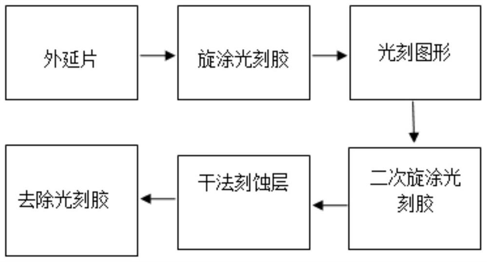
[0057] Step 1: Prepare the chip first;

[0058] Step 2: spin-coat photoresist again, and spin-coat a layer of positive photoresist on the surface of the prepared chip epitaxial wafer to form a photoresist layer; then bake the chip to remove the solvent in the photoresist; The thickness of the resist layer is

[0059] Step 3: Then use the photolithographic mask to expose the photoresist layer, and then remove the exposed part of the photoresist by developing, and photoetch the required pattern photoresist on the epitaxial wafer, wherein the photolithographic mask The pattern width in is 10 μm;

[0060] Step 4: Put the treated chips in an oven and bake at 90°C for 5 minutes;

[0061] Step 5: Next, spin-coat the photoresist for the second time, take the baked chip, and spin-coat a layer of positive photoresist on the surface of the photoresist layer to form a photoresist mask layer with a groove-shaped radian; The chip is baked again to remove the solvent in the photoresist;...

Embodiment 2

[0066] Step 1: Prepare the chip first;

[0067] Step 2: spin-coat photoresist again, and spin-coat a layer of positive photoresist on the surface of the prepared chip epitaxial wafer to form a photoresist layer; then bake the chip to remove the solvent in the photoresist; The thickness of the resist layer is

[0068] Step 3: Then use the photolithographic mask to expose the photoresist layer, and then remove the exposed part of the photoresist by developing, and photoetch the required pattern photoresist on the epitaxial wafer, wherein the photolithographic mask The pattern width in is 18 μm;

[0069] Step 4: Put the treated chips in an oven to bake, the baking temperature is 100°C, and the baking time is 10 minutes;

[0070] Step 5: Next, spin-coat the photoresist for the second time, take the baked chip, and spin-coat a layer of positive photoresist on the surface of the photoresist layer to form a photoresist mask layer with a groove-shaped radian; The chip is baked ag...

Embodiment 3

[0075] Step 1: Prepare the chip first;

[0076] Step 2: spin-coat photoresist again, and spin-coat a layer of positive photoresist on the surface of the prepared chip epitaxial wafer to form a photoresist layer; then bake the chip to remove the solvent in the photoresist; The thickness of the resist layer is

[0077] Step 3: Then use the photolithographic mask to expose the photoresist layer, and then remove the exposed part of the photoresist by developing, and photoetch the required pattern photoresist on the epitaxial wafer, wherein the photolithographic mask The pattern width in is 25 μm;

[0078] Step 4: Put the treated chips in an oven and bake at 110°C for 15 minutes;

[0079] Step 5: Next, spin-coat the photoresist for the second time, take the baked chip, and spin-coat a layer of positive photoresist on the surface of the photoresist layer to form a photoresist mask layer with a groove-shaped radian; The chip is baked again to remove the solvent in the photoresis...


PUM


Abstract

The invention discloses a preparation method of a small-size groove. The method comprises the following steps of spin-coating a layer of thick positive photoresist on an epitaxial wafer, preparing a photoresist window with a certain width by using a photoetching mask plate in an exposure and development mode, and directly spin-coating a layer of thin photoresist on a sinking bottom with the photoresist to obtain the small-size groove; a photoresist mask layer with a trench radian being formed, the size of the bottom of the trench radian being smaller than the width of a photoresist developmentpattern, finally, thin photoresist at the bottom of a trench being etched away through dry etching, etching continuing to be conducted directly with the photoresist as a mask, a trench pattern with the size smaller than or equal to 5 micrometers being obtained, and preparation of a trench with the smaller sizebeing achieved. The method is advantaged in that the method is reasonable in design andsimple to operate, the preparation of the small-size trench is effectively realized, multiple times of photoetching are avoided, the preparation can be realized by direct one-time dry etching, meanwhile, use cost is low, process steps are simplified, and practicability is better.

Description

technical field [0001] The invention relates to the technical field of semiconductors, in particular to a method for preparing small-sized grooves. Background technique [0002] At present, the demand for bar chips is increasing. Since the length of bar chips is generally 1cm, in order to reduce the current density of the die, it is necessary to increase the luminous points of the entire bar, which will reduce the size of a single chip. In order to avoid interference between individual dies inside the bar, it is necessary to prepare grooves between the dies. At the same time, in order to use the entire bar most effectively, the light-emitting area of ​​a single die should be as large as possible, and the width of the groove should be as small as possible, which requires higher photolithography technology. However, in the photolithography process, especially the preparation process of small-sized patterns, how to accurately copy the small-sized patterns onto the photoresist ...

Claims


Application Information

Patent Timeline
Patent Type & Authority Applications(China)
IPC IPC(8): G03F7/16G03F7/20G03F7/40H01L21/768H01L21/3065
CPCG03F7/162G03F7/168G03F7/2024G03F7/40H01L21/3065H01L21/76802
Inventor 王金翠苏建任夫洋陈康吴萌萌
Owner Shandong Huaguang Optoelectronics Co. Ltd.
Why Eureka
Try Eureka